SED, secondary electron detector, SE detector, ET detector
SED, secondary electron detector, SE detector, ET detector
The most widely used secondary electron (SE) detector is the ET (Everhart-Thornley) detector, which is composed of a scintillator and a photomultiplier tube (PMT). The name of the ET detector is originated from the inventors of this detector, Everhart and Thornley.
In a general-purpose SEM, the specimen is placed outside (underside) of the objective lens, and the ET detector is attached in the space between the objective lens and the specimen (on the side part of the specimen chamber). Figure below shows the construction of the ET detector and the positional relation between the objective lens and specimen.
The surface of the scintillator, which is made of powders of yttrium silicate, is aluminum (Al) coated. An electrode (called “collector”) is placed in front of the scintillator.
A voltage up to several 100 V can be applied to the collector. The electric field generated by the applied voltage collects the secondary electrons emitted from a specimen. Those electrons guided to the scintillator are further accelerated by a high voltage of +10 kV applied to the Al-coated film of the scintillator and hit the scintillator, causing light emission. The emitted light is guided to a PMT through a light guide tube, and converted back to electrons and are multiplied. The multiplied electrons arrive at the anode and are converted to a voltage signal and amplified by the electric circuit connected to the PMT.
In a high-resolution SEM, the specimen is placed in (or close to) the objective lens. Thus, secondary electrons are generated in (or enter) the objective lens. To collect these secondary electrons, the ET detector is placed inside the microscope column.
The ET detector, which is widely used as the SE detector, has a high response speed because it uses a scintillator like the yttrium aluminum garnet (YAG) detector. Therefore, the image of the specimen can be observed with no blurring and without time lag even at fast scanning or moving the specimen stage.
It is noted that for detecting backscattered electrons, a silicon (Si) semiconductor detector is mainly used but a YAG detector is used when a high response speed is required.
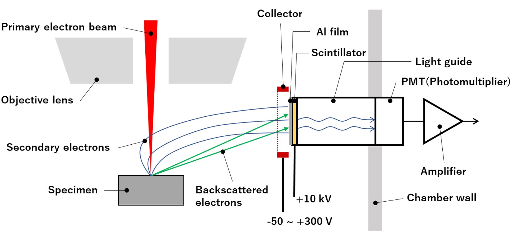
Fig. Secondary electron detector (ET detector)
Secondary electrons emitted from a specimen are guided to the SE detector (ET detector) by the collector. The guided secondary electrons are converted to light by the scintillator and converted back to electrons by the PMT, where they are amplified and become an electric current. The electric current is converted to a voltage signal and amplified by the connected electrical circuit. The surface of the scintillator is aluminum-coated for preventing the deterioration of the surface caused by discharge. It is noted that a few amounts of backscattered electrons are also detected with the ET detector.
The scintillator is made of powdered yttrium silicate, which is less expensive than crystalline YAG.
Term(s) with "SED, secondary electron detector, SE detector, ET detector" in the description

Are you a medical professional or personnel engaged in medical care?
No
Please be reminded that these pages are not intended to provide the general public with information about the products.


