Atomic-Resolution Characterization Using the Aberration-Corrected JEOL JEM-ARM200CF at the University of Illinois – Chicago
JEOLnews Volume 49, Number 1, 2014
Robert F Klie, Ahmet Gulec, Arijita Mukherjee, Tadas Paulauskas,
Qi ao Qi ao, Xue Rui , Runzhe Tao, Canhui Wang , Tad Dani e l ,
Patrick J. Phillips, Alan W. Nicholls
University of Illinois at Chicago
Modern aberration-corrected scanning transmission electron microscopes (STEM) provide a multitude of characterization techniques that can be applied across a wide-range of length and temperature scales. At the University of Illinois at Chicago, the aberration-corrected, cold-field emission JEOL JEM-ARM200CF is capable of atomic-resolution imaging, electron energy-loss (EEL) as well as energy-dispersive X-ray (XEDS) spectroscopy in a temperature range between 80 – 1,300 K. The capabilities of this instrument will be demonstrated using a number of studies focusing on both structural and chemical properties of materials including NbH, SrTiO3, CdTe and ferritin protein. The central theme of these studies is microscope versatility, which is realized through the ability to perform atomic-scale chemical characterization while retaining high spatial imaging resolution. Of particular interest to many studies is the visualization of light elements, such as N, O or H, using simultaneous high-angle annular dark field (HAADF) and annular bright field (ABF) imaging. Novel insitu capabilities will be demonstrated using graphene liquid cells. Finally, we will demonstrate the effects of a new silicon drift detector, the Oxford X-MaxN 100TLE on performing atomic-column resolved XEDS mapping at varying length scales and energy resolution.
Introduction
A better understanding of the mechanisms that influence a material’s property on the atomic level is essential for developing new functional nano-devices for electronics, energy and biological applications, it is essential that we gain an understanding. Even more so than on the macroscopic level, when a component has been miniaturized for use in nano-devices, surfaces, interfaces, and individual defects dominate its properties by changing the material’s structural, compositional and bonding behavior. If working and reliable devices are to be successfully fabricated, it is imperative that we understand the structure-property relationships of these defects, interfaces and surfaces.
Over the last decade, analytical transmission electron microscopy (TEM) and scanning TEM (STEM) have emerged as the primary tools for exploring the structure-property relationships of novel nano-materials [1-15], in particular the atomic and electronic structures of defects, interfaces, or nano-particles [16-20] . The scanning transmission electron microscope (STEM) fitted with a probeside aberration corrector, such as the JEOL JEM- 2200FS or the JEOL JEM-ARM200F [21-24] yields unparalleled spatial resolution of both heavy and light chemical species. With spatial resolution of aberration-corrected high-resolution phase contrast imaging (HRTEM) and high angle annular dark field, HAADF, (or Z-contrast) imaging in aberrationcorrected STEMs now reaching the fundamental limit of the Bohr radius, a0~ 50 pm, the focus is shifting to increasing the chemical resolution and visualizing all constituent atomic species , while retaining spatial resolution. To that end, electron energy loss spectroscopy (EELS) and energy-dispersive X-ray spectroscopy (XEDS) are being pushed to the point where atomically-resolved chemical maps are possible with both techniques [25, 26]. The implementation of silicon drift detectors (SDD) with larger active detector areas in XEDS have greatly aided this advancement, leading to the demonstration of single atom sensitivity [27]. Many material systems are utilized in devices under conditions (i.e. temperatures, pressures or fields) that are substantially different from those present inside an electron microscope column. In a conventional atomic-resolution transmission electron microscope, atomic-resolution studies have previously been limited to ambient temperatures and under high vacuum (PO2=10-5 Pa) due to the inability to get in-situ holders into the small gap of an ultrahigh- resolution objective lens pole-piece. Over the last decade, the field has advanced significantly, and in-situ capabilities are now available to study the dynamic behavior of materials in environments other than the high-vacuum of the TEM column. Novel sample stage designs have enabled in-situ heating up to 1,300 K with atomic resolution, in-situ gas and liquid experiments with nano-meter resolution, as well as time-resolved imaging with better than nanosecond resolution. This paper will demonstrate the capabilities of the JEOL JEM-ARM200CF at the University of Illinois at Chicago, a probe aberration-corrected STEM equipped with a cold-field emission electron source, a post-column EEL spectrometer and the new Oxford X-MaxN 100TLE SDD-XEDS detector. We will demonstrate that atomic-resolution imaging of light elements, including N, O and H is possible using ABF imaging, while the cold-field emission electron source allows for EELS with an energy resolution of better than 400 meV. In addition, we will highlight our newly developed graphene liquid cell approach of encapsulating biological samples, such as ferritin proteins in a liquid between two single layers of graphene.
Experimental
The JEOL JEM-ARM200CF installed in the Research Resources Centre (RRC) at the University of Illinois at Chicago (Fig. 1) is equipped with a cold field emission gun, 5 annular detectors, a Gatan Enf ina EELS spectrometer and the new Oxford X-Ma xN 10 0TLE SDD EDS detec tor and was installed in our laboratory in late 2011. The spatial resolution that can now be routinely achieved using the JEOL JEM-ARM200CF exceeds 70 pm at 200 kV primary energy (see Fig. 2(a)) and 100 pm at 80 kV primary energy. The energy resolution of the EEL spectra at any energy between 80 and 200 kV is 350 meV (see Fig. 2(b)). The stability of the instrument was measured using a long-exposure HAADF image without dr if t correction, and was determined to better than 150 pm/min. In addition to the double tilt holders, we also took delivery of a Gatan doubletilt liquid He cooling stage, a Protochips Aduro double tilt heating stage, a Fischione tomography stage, as well as a Nanofactory STM-TEM stage and a Protochips Poseidon liquid flow cell. In addition, we have still access to the Gatan double tilt heating and the double tilt LN2 cooling stage, which were purchased in 1998 for use in the UIC JEM-2010F.
In this paper, we will show results from several of these in-situ stages, including the Gatan LN2 cooling stage and the home-made graphene liquid cell. These results are meant to demonstrate the wide range of experiments that can be conducted on a daily basis in the ARM200CF. At this point, it is important to note that switching between TEM and STEM mode can be done without disturbing the alignment or stability of the instrument significantly. For example, when switching from TEM to STEM mode, it is possible to achieve atomic resolution nearly immediately after the coma and astigmatism have been manually corrected. At the highest imaging resolution, we notice that during the first 60-120 minutes after entering STEM mode, some adjustment of the focus and stigmator is necessary. Once the ARM200CF has been in STEM mode for two hours, the instrument is completely stable.
The UIC JEOL JEM-ARM200CF is located in an open-access user-facility, which allows qualified users to use the instrument 24 hours, 7 days per week on an hourly user-charge basis [28]. It is, therefore, crucial that any of the experimental setups required by the user are not affecting the performance of the instrumentation for the subsequent users. To date, we have not experienced any significant influence of any in-situ experiments or low-voltage measurements on the vacuum column or energy-stability performance for more than a few hours after the completion of the experiments.
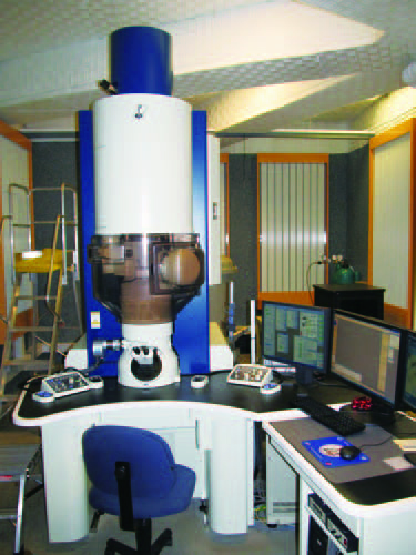
Fig. 1 The JEOL JEM-ARM200CF at the University of Illinois at Chicago.
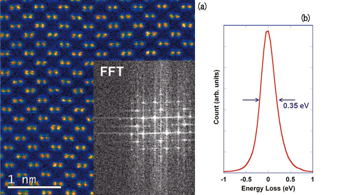
Fig. 2 a) HAADF image at 200 kV of Si (110) with Fourier transform shown as insert. b) Zero-loss peak with indicated full width at half maximum.
Results and Discussion
Here, we will discuss the results from several experiments conducted using the JEOL ARM200CF at the University of Illinois at Chicago. The materials that were characterized include SrTiO3 thin films on GaAs, ß-NbH, polycrystalline CdTe and ferritin proteins in a graphene liquid cell.
Low voltage characterization of SrTiO3/GaAs interfaces
Over the past few years, ultrathin metal-oxide films on polar semiconductor surfaces have received much at tent ion due to the occurrence of novel inter facial proper ties, including ferroelectricity, superconductivity and the presence of an interfacial 2 - dimensional electron gas [29 -34] . The first successful growth of SrTiO3 thin films on Si was reported more than two decades ago, and various techniques have been used to assemble a layer-bylayer crystalline oxide film and avoid the formation of the amorphous layer at the interface [35, 36].
The SrTiO3 /GaAs inter faces were studied experimentally and theoretically with various techniques in order to develop a fundamental understanding of the structure property relationships and it has been reported that the SrTiO3 film prefers to be SrO terminated at the interface, regardless of the growth condition, and a submonolayer of Ti, hereafter referred to as a Ti pre-layer, between the oxide and semiconductor can release the Fermi level pinning after the thin film deposition.[37-39] However, due to the oxygen deficiency of the film, it was not possible to per form atomic resolution electron energy-loss spectroscopy (EELS) on the highly beam sensitive SrTiO3/GaAs interface [40].
Using the JEOL ARM200CF at UIC, we conducted a detailed study of the atomic and electronic structures of the SrTiO3/GaAs interface with and without a Ti pre-layer using HAADF imaging and EELS at 80 kV primary electron energy [41] . Figure 3 shows atomic-resolution Z-contrast images of a 4 monolayer thin SrTiO3 film on GaAs (001), where the epitaxy is apparent with SrTiO3(001) || GaAs (001) and SrTiO3[110] || GaAs [100] . The interface between the SrTiO3 film and the GaAssuppor tin Fig. 3 appears sharp with no obvious interfacial diffusion. Moreover, the images suggest that the oxide films start with a SrO layer at the As terminated GaAs interface, regardless of the fact that 0.5 ML of a Ti pre-layer was deposited on the GaAs surface prior to SrTiO3 growth for the sample shown in Fig. 3(a)). As opposed to the experiments conducted at 200 kV primary electron energy, the SrTiO3/GaAs interfaces are now sufficiently stable to withstand atomic resolution imaging and spectroscopy for extended periods of time. Even several hours of analysis on a particular region of a sample has so far not shown any signs of beam damage, neither in Z-contrast imaging nor in spectroscopy.
The acquired Ti L- and O K-edges are shown in Fig. 4 and Fig. 5, respectively acquired using a convergence semi-angle of 30 mrad, a collection semiangle of 35 mrad, with a 0.1 eV/pxl dispersion and a 3s dwell time. The top spectrum in Fig. 4 and Fig. 5 is taken from a SrTiO3 bulk specimen thus providing a Ti4+ fine structure as a reference. In Fig. 4, the crystal field splitting of Ti L3 and L2 edges can be clearly resolved in all the spectra taken from the SrTiO3 thin film, which indicates that the Ti valence is close to 4+ throughout the films in both films with and without the Ti prelayer.[42] To further assess the Ti valence state, and thereby the oxygen stoichiometry of the films, the energy scale has been calibrated using the O K-edge onset, as shown in Fig. 4.
It can now be seen that in the film without the Ti pre-layer, the Ti L-edges for each location in the film are slightly shifted towards lower energy, again indicating a slight decrease in the Ti. More specifically, both L3 and L2 edges shift to lower energies as the electron probe approaches to the SrTiO3/GaAs interface, indicating a decrease of the Ti valence from 4+ to a mixture state of 3+ and 4+ [42] . Such phenomena could be caused by oxygen vacancies, or because the Ti-O bonding state on the TiO2 columns in the thin film changed to Ti-As on the surface of the substrate. In addition, it is interesting to note here that a Ti signal is noticeable at least 2 layers into the GaAs support, indicating that some of the Ti has diffused into the GaAs support during the film synthesis. In Fig. 5, the acquired O K-edges are fitted to their 5th nearest neighbors and compared with the reference spectrum taken from bulk SrTiO3. The colored spectra cor respond to the colored rectangles in Fig. 3. It is immediately noticeable that the O K-edge fine-structure in the SrTiO3 thin films is significantly different from the bulk SrTiO3, especially for the film grown without the Ti prelayer. More specifically, the pre-peak, which strongly scales, with the presence of oxygen vacancies, is suppressed in the spectra taken from the films [43, 44], indicating the presence of oxygen vacancies. Furthermore, near the SrTiO3/GaAs interface, the fine-structure of the O K-edge exhibits several peaks that were not found in the bulk SrTiO3, nor in the films SrTiO3 spectra. These additional peaks indicate the oxygen bonding with arsenic on the GaAs surface during the initial steps of the thin film synthesis. Finally, the integrated O K-edge intensity disappears completely in the GaAs support, even in the locations where a Ti signal was found. This further indicates that only the Ti diffuses into the support, while the oxygen remains in the SrTiO3 film and on the GaAs surface.
Our low-kV imaging and spectroscopy study, therefore, shows, that while the atomic structure of the interfaces does not reveal any evidence of the Ti prelayer at the SrTiO3 interface, the electronic structure of the films appears significantly different. The films grown without the Ti pre-layer appears to be more oxygen deficient , and exhibit stong interact ion between the GaAs support and the interfacial oxygen, potentially forming As2O3. The deposition of the Ti pre-layer appear to alleviate the oxidation of the substrate and consequently lift the Fermi-level pinning [41].
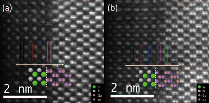
Fig. 3 Atomic resolution HAADF image at 80 kV of SrTiO3 /GaAs a) with and b) without the Ti pre-layer.
The colored rectangle highlight the area where EEL spectra where acquired. An atomic model is superimposed on the images and the interface is indicated by the dotted line.
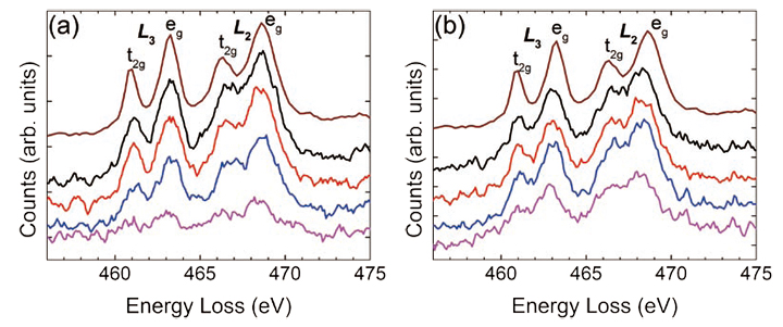
Fig. 4 EELS at 80 kV of the Ti L-edges after background subtraction for the sample a) with and b) without the Ti pre-layer.
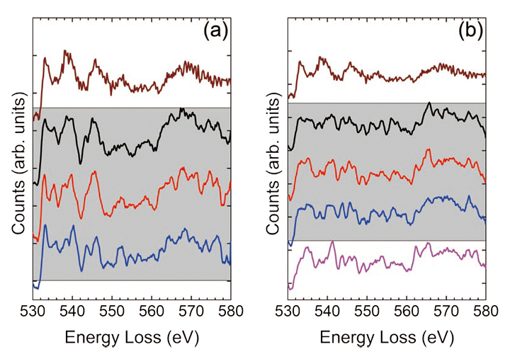
Fig. 5 EELS at 80 kV of the Ti L-edges after background subtraction for the sample a) with and b) without the Ti pre-layer.
EELS spectra of the O K-edges for the samples a) with and b) without the Ti pre-layer. The shaded area indicates spectra taken from the SrTiO3 film, while the top spectrum is taken from bulk SrTiO3 as a reference.
Direct imaging of hydrogen in ß-NbH
Niobium, a 4d trans it ion metal , has found many appl icat ions including hydrogen storage, heterogeneous catalysis, dielectric coatings, and superconducting devices, such as superconducting radio-frequency (SRF) cavities [45] . In the next generation accelerators, the performance of SRF cavities at moderate (i.e. 16-19 MVm-1) and high electric (i.e. >35 MVm-1) field gradients are critical [46]. Nevertheless, even after decades of research, a solid understanding of the microstructural defects limiting the medium and high field performance is still missing. What appears clear, however, is that Niobium hydride, if present, can be a major contributor to the deg radation of the qua l it y factor, Q, since hydride precipitates can only be superconducting by proximity effect , and their premature transition to the normal state will lead to strong losses [47, 48].
Here, we present an atomic-resolution study of the formation of ß-NbH precipitates at room temperature in Nb grains near the cavity surfaces. [49] In addition, we demonstrate that atomic-resolution imaging is still possible at LN2 temperatures, although spatial drift limits the dwell time per pixel to around 16 μs/pixel.
Figure 6 shows a pair of HAADF and ABF images , acquired simultaneously, of a ß-NbH precipitate in the [110] orientation. While the HAADF image appear s very similar to that of pure Nb, the ABF image reveals additional atomic columns, which can be identified as hydrogen atomic columns. The insert in Fig. 6 shows the proposed structure of ß-NbH [110] as well as the calculated image contrast using the multi-slice method. The contrast in the image calculations agrees with that measure in the experimental ABF images. Using a combination of ABF imaging, selective area electron diffraction and EELS, we confirmed that the phase image is ß-NbH [110].
According to the phase diagram for Nb-hydride, there exist several other phases depending on the local hydrogen concent rat ion and temperature. Therefore, in order to fully understand the role of hydride precipitates on the mid and high field gradient performance of Nb based SRF cavities, an imaging method capable of atomic-resolution at low temperature (e.g. LN2 temperature) is needed. Using the Gatan double tilt LN2 stage, we imaged bulk Nb [110] (Fig. 7(b)) and show that achieving atomicresolution is possible at that temperature. However, due to the increase mechanical vibrations as a result of the nitrogen boiling off, we had to decrease the pixel dwell time to 16 μs /pixel and average over several images to achieve a presentable signal to noise ratio. If necessary, more sophisticated noise reduction procedures can be employed if repeated acquisition of short-exposure time images is not possible.
![Fig. 6 Simultaneous HAADF and ABF images at 200 kV of ß-NbH [110] clearly showing the hydrogen atomic columns in the ABF image.](./product_file/file/e49_02-fig6.jpg)
Fig. 6 Simultaneous HAADF and ABF images at 200 kV of ß-NbH [110] clearly showing the hydrogen atomic columns in the ABF image.
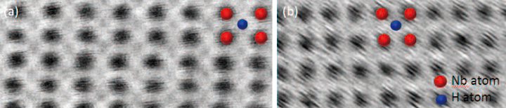
Fig. 7 200 kV atomic-resolution ABF images at a) room and b) LN2 temperature. Both images show the Nb atomic columns, but the Hydrogen columns are not very visible in the low temperature image due to the increased sample vibration.
XEDS analysis of defects in polycrystalline CdTe
Polycrystalline CdTe thin film based photovoltaic devices are present leaders in thin film solar technology ([50] , [51]). Commercial success of CdTe based devices stems from the nearly ideal band gap of the material which very effectively couples to our sun’s light spectrum as well as ease of manufacturing and low cost of the modules. However, to improve the conversion efficiency beyond 20%, it is critical to minimize the harmful effects of grain boundaries and lattice defects in CdTe. Direct atomic-scale structural and chemical investigation is desirable in order to identify atomic configurations which can act as carrier recombination centers. Likewise, it is necessary to confirm that passivants introduced into CdTe are able to diffuse and bind to the target defects. Besides arbitrarily oriented grain boundaries, stacking faults and Ʃ3 twin boundaries, both lying on {111} planes, are very common planar defects in CdTe. These defects have the cor rect nearest-neighbor bonding, however stacking disorder becomes apparent in second (and beyond) nearest neighbors. While these interfaces have been deemed benign as far as carrier recombination centers are concerned, their role in attracting impurities and anti-site point defects remains unknown. In Fig. 8, we show an HAADF image and XEDS image of a stacking fault in CdTe along [110] . In this projection, Cd and Te atomic columns form a dumbbell-like structure with 162 pm column separation. The XEDS data clearly shows atomic resolution and the polarity of the planar defect can be readily identified. More precisely, the direction of the dumbbells at the stacking fault is rotated by 250° about [110]. Figure 8 shows that the terminating column of the left side of the interface is Te, followed by Cd. Such data will allow us to quantify possible changes in stoichiometry across twin boundaries and stacking faults, detect the presence of dopants, and determine the atomic structure of dislocation cores terminating such defects.
HAADF image and atomic-column resolved XEDS map of a Lomer-Cottrell dislocation along [-1- 10] zone-axis in CdTe are presented in Fig. 9. More specifically, two intrinsic stacking faults are seen in the HAADF image and the XEDS spectrum image shows the integrated intensity of the Cd and Te L-peaks in the stacking faults. The dislocation core is located at the vertex of two intersecting stacking faults, and is composed of three Cd atomic columns and a single Te column (Cd3Te), as can be seen from the spectrum image map shown in Fig. 8. It should be pointed out here that without the availability of the XEDS spectrum image, the identification of the atomic columns in the dislocation core would not be possible, since the atomic numbers (Z) for Cd and Te are too close to be distinguished using HAADF imaging alone.
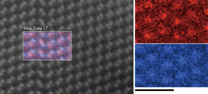
Fig. 8 An HAADF STEM image acquired across a twin boundary, viewed with the Cd L (red) and Te L (blue) series overlaid. The scale bar is 1 nm and applies to the individual element maps.
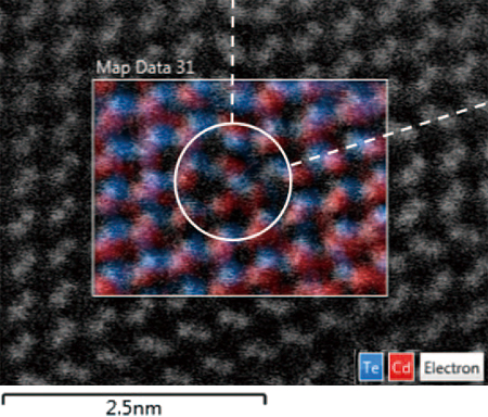
Fig. 9 a) Atomic-column resolved XEDS map overlaid on top of the Z-contrast image in the <110> projection. L-C dislocation core (circled) is associated with the two dashed intrinsic stacking faults.
Ferritin in a graphene liquid cell
Nanoparticle growth, chemical reactions or biochemical activity often occur in the presence of a liquid. To study liquid sample in an electron microscope, several liquid cell designs have become commercially available in recent years that enable materials to be imaged in a carefully controlled liquid environment within the vacuum of a TEM. However, all suffer from a few key limitations that do not allow for ultra high-resolution imaging or spectroscopy:[52] 1) two Si3N4 layers (50-500 nm thick) used as electron transparent windows and 2) the thickness of the liquid surrounding the sample. In these liquid cells, the imaging resolution is usually limited to nanometers. Electron energy-loss spectroscopy (EELS) is degraded by multiple scattering events in the thick window layers, and the strong coreloss signals associated with the presence of Si and N [53]. In addition to the increased sample thickness, radiation damage is a fundamentally limiting factor when examining beam sensitive materials and /or hydrous samples in TEM. It has been shown that coating the specimen with carbon, metal or grapheme [54-58] , or lowering the temperature [57] have positive effects against radiation damage by reducing electrostatic charging, mass loss, loss of crystallinity, or defect format ion rate [54-58] . These studies suggest that it is possible to reduce radiation damage to below breakage of covalent bonds. However, further reduction of radiation damage is needed for characterization of biological samples, since many biological structures and functions are related to the much weaker hydrogen bonds.
We have developed a biocompatible approach of encapsulating liquid containing samples in monolayers of graphene. This not only a l lows biological samples to be directly imaged at atomic resolution in a native liquid state without limitations from the window thickness (see Fig. 10), but also enables nm-scale analysis using EELS to quantify reactions in an aqueous environment [59]. It has to be pointed out here that any imaging or chemical analysis of graphene liquid cells required that the electron beam energy is lowered below 100 kV, and the images shown in Fig. 10 are taken at 80 kV.
Further, we have shown that the energy deposited by the incoming electrons is dissipated by graphene from the area irradiated at a rate equivalent to the beam current of several electrons per Å2 per second [59]. This would therefore provide a reduction of radiation damage, allowing for high resolution imaging and spectroscopy of beam sensitive materials. Details, such as individual Fe atoms (see Fig. 10) or polypeptide of unstained protein, are resolved in a liquid environment. By carefully controlling the induced electron dose rate, we have shown that react ions, such as liquid / gas phase transition (bubble formation and condensation), or nanoparticle / nanowire growth can be initiated at selected locations in GLC, and recorded at nm resolution. This technique also allows us to perform a quantitative study of radiation damage effect on different encapsulated samples, such as water or protein, by observing local reaction processes.
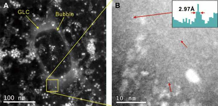
Fig. 10 HAADF (A and B) images of ferritin in a graphene liquid cell (GLC). Bubbles in (A) were formed in advance using the Ronchigram mode to confirm the presence of a liquid. In STEM mode, electron dose rate and pixel dwell time is optimized so that no further bubbles are formed during scanning. Single iron atoms are resolved in a liquid environment in image (B) near the edge of a GLC. A line profile across the upper left atom is shown as an inset of (B), with each pixel corresponds to 0.99 Å. The resolution of these images is optimized by taking images under the corresponding threshold area averaged dose rate of bubble formation at each magnification.
Conclusion
Nearly two years after the delivery of the new JEOL ARM200CF to UIC, we have demonstrated the capabilities of the instrument to perform with sub-Å and sub-eV resolution in a variety of environments using a 200 kV primary energy electron beam. The spatial resolution is decreased in 1.0 Å for low energy imaging at 80 kV without any loss in the analytical capabi l it ies of the inst rument . In addit ion, the ARM200CF is capable of imaging samples in a liquid environment, at elevated or cryogenic temperatures in either TEM or STEM mode.
Acknowledgments
The author s acknowledge suppor t for thi s work from the National Science Foundation [DMR- 0846748] and the US Department of Energy (DOEEE0005956). The acquisition of the UIC JEOL JEMARM200CF is supported by a MRI-R2 grant from the National Science Foundation [DMR-0959470]. Support from the UIC Research Resources Center is also acknowledged.
References
[ 1 ] Hashimoto, A., et al., Direct evidence for atomic defects in graphene layers. Nature, 430(7002): p. 870-873 (2004).
[ 2 ] Regan, B.C., et al., Carbon nanotubes as nanoscale mass conveyors. Nature, 428(6986): p. 924-927 (2004).
[ 3 ] Cumings, J., P.G. Collins, and A. Zettl, Materials - Peeling and sharpening multiwall nanotubes. Nature, 406(6796): p. 586-586 (2000).
[ 4 ] Iijima, S., Helical Microtubules of Graphitic Carbon. Nature, 354(6348): p. 56-58 (1991).
[ 5 ] Wang, Z.L. and Z. Kang, C., Functional and Smart Materials.: Plenum Press (1998).
[ 6 ] Ohtomo, A., et al., Artificial charge-modulation in atomic-scale perovskite titanate superlattices. Nature, 419(6905): p. 378-380 (2002).
[ 7 ] Zuo, J.M., et al., Atomic resolution imaging of a carbon nanotube from diffraction intensities. Science, 300(5624): p. 1419-1421 (2003).
[ 8 ] Bell, A.T., The impact of nanoscience on heterogeneous catalysis. Science, 299(5613): p. 1688-1691 (2
お問い合わせ
日本電子では、お客様に安心して製品をお使い頂くために、
様々なサポート体制でお客様をバックアップしております。お気軽にお問い合わせください。