Photonic Crystal Lasers
JEOLnews Volume 49, Number 1, 2014
Susumu NODA
Department of Electronic Science and Engineering, Kyoto University
In this article, recent progress in broad-area photonic-crystal lasers based on photonic bandedge effect is described. It is shown that unique beam patterns can be generated by designing photonic crystal structures. Moreover, it is demonstrated that watt-class high-power, high-beamquality, surface-emitting, lasing oscillation has been successfully achieved. These results represent an important milestone for innovation in the field of lasers because it provides a route towards overcoming limitations in applications that suffer from low beam quality, which opens the door to a wide range of applications in material processing, laser medicine, nonlinear optics, sensing and so on.
Introduction
It is well known that semiconductor distributed feedback lasers possess a one-dimensional lattice, and that the forward-propagating wave undergoes Bragg reflection due to this grating, being diffracted to the opposite direction. The resulting forward and backward-propagating waves couple with each other to generate a standing wave, forming a cavity. This is equivalent to the fact that in a one-dimensional photonic crystal the cavity loss is smallest at the band edges, which are at both ends of the photonic bandgap, giving rise to a state that causes oscillation. When this idea is extended to photonic crystals with two-dimensional per iodicity, one can make use of the coupling of optical waves due to Bragg reflection within the two-dimensional plane in order to form a standing wave state that covers the entire surface of the plane [1,2] . As a result, it becomes possible to obtain an oscillation mode with an electromagnetic field distribution that is perfectly defined at each lattice point in the two-dimensional crystal. The optical output can be diffracted in the direction perpendicular to the plane of the crystal, thus realizing a sur face-emitting character istic. Two-dimensional photonic crystals hence enable the construction of surface-emitting lasers in which not only the longitudinal mode of lasing is defined, but also the beam pattern, usually referred to as the transverse mode. Furthermore, it becomes possible to realize a novel laser that oscillates in a single longitudinal and transverse mode, no matter how large the surface area is, which surpasses a conventional concept in the field of laser research.
The first semiconductor laser to be based on this principle was realized in 1999 [1] . Since then, in addition to the demonstration of roomtemperature continuous lasing, it has been shown that two-dimensional photonic crystals can generate beams with controlled polarization and patterns; for example, a doughnut-shaped beam can be formed, which is expected to be focusable to sizes smaller than the wavelength [2-6]. The other notable recent developments using this principle are the realization of a current-injection-type blue-violet surface-emitting operation and electronically beam-steering operation [7, 8]. We discuss the current state of the art in the following sections.
Basic Device Structure and Operation Principle
Figure 1 shows an example of a laser based on the two-dimensional photonic crystal band-edge effect. This laser consists of two wafers, A and B; wafer A includes an active layer for the injection of electrons and holes, and a photonic crystal as the upper-most layer. The integration of wafers A and B results in the photonic crystal being sandwiched to complete the device. As shown in the insert of Fig. 1, this photonic crystal has a square lattice structure and is designed such that the periodicity in the Г-X direction matches the emission wavelength in the active layer. In this design, light propagating in a certain Г-X direction is Bragg diffracted to the opposite (-180°) direction, as well as to the -90° and 90° directions; the four equivalent light waves propagating in the Г-X direction then couple to form a two-dimensional cavity. More precisely, higherorder Bloch waves in addition to these fundamental four waves are involved for the construction of twodimensional cavity mode (see Fig. 2(a)). Figure 2(b) shows the photonic band structure of this cavity. The lasing mode occurs at the band edges indicated by the red dots at the Г-points of the four bands, A, B, C and Kyoto 615-8510, Japan, E-mail: snoda@kuee.kyoto-u.ac.jp (2014) Vol. 49 No. 1 JEOL News 30 D. Detailed analysis [9] indicates that either of band edges in bands A and B yields the highest Q factor, and that lasing oscillation most readily occurs there. The output beam can be coupled out to the direction normal to the photonic crystal surface.
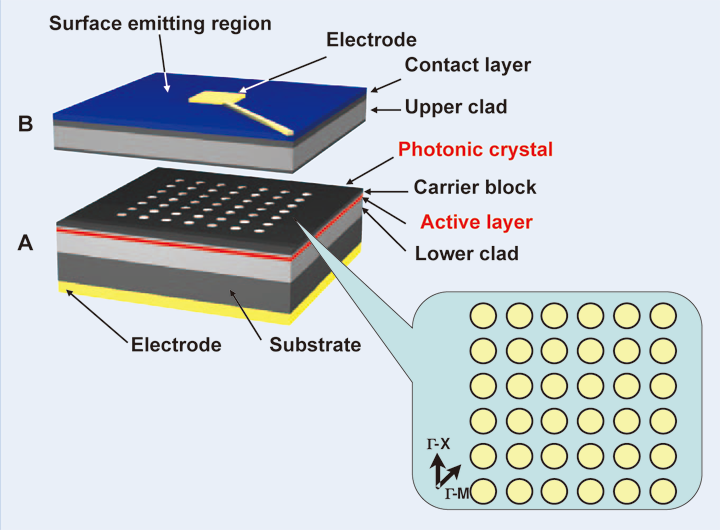
Fig. 1 Schematic of an example of a laser based on the twodimensional photonic crystal band-edge effect. The inset shows the photonic crystal with a square lattice structure.
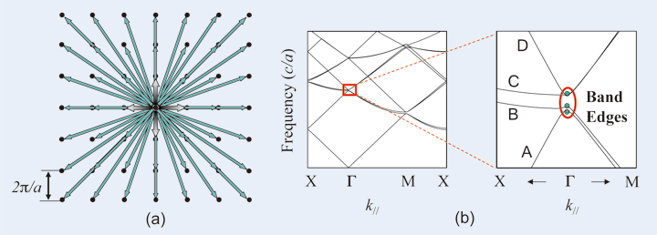
Fig. 2 (a) Bloch waves which construct a two-dimensional cavity mode, and (b) photonic band structure.
Broad Area Coherent Oscillation and Beam Pattern Control
To construct the device shown in Fig.1, the photonic crystal was fabricated by electron beam lithography and dry etching technique and embedded in the device by a wafer bonding technique. The device successfully oscillated coherently in the broad area as shown in Fig. 3. It is apparent that a singlewavelength operation was achieved across the device despite the large lasing area of 150 × 150 μm.
Such an ability to realize broad-area coherent oscillation enables us to produce very unique beam patterns, which cannot be realized by conventional semiconductor lasers. Because the pattern of the surface-emitted beam from a photonic crystal laser can be determined by the Fourier transformation of its two-dimensional electromagnetic distribution, the beam pattern can be tailored by varying the electromagnetic distribution in the two-dimensional plane, that is, by changing the coupling state of the light that propagates in various directions in the twodimensional plane. One effective method of achieving this is to vary the shapes and spacing of the lattice points in the photonic crystal. Figure 4(a) and (b) show the electromagnetic field distribution in the unit lattice of a crystal when the holes placed at the lattice points are circles and equilateral triangles, respectively. Changing the shape of the holes from circular to triangular removes the four-fold rotational symmetry in the electromagnetic field distribution; there is no symmetry in the x-direction for triangular holes. Figure 4(c) – (g) show the electromagnetic field distributions over the entire crystal in cases where shifts of the lattice points were introduced in order to increase the lattice spacing in either the longitudinal or transverse directions. Figure 4(c) represents the case with no shift, whereas Fig. 4(d) – (g) represent increasing numbers of shi f ts. It is apparent that shifting the lattice spacing reverses the polarity of the electromagnetic field distribution at the position of the shift. Further increasing the number of shifts repeats the reversal of the electromagnetic field. It is clear that the electromagnetic field distribution in the plane can be controlled in various ways by appropriate design of the photonic crystal.
We fabricated devices with various different photonic crystal structures , as shown in Fig. 5 (a) –5(f) . All of these devices exhibited lasing oscillation at room temperature with a stable single mode. The right-hand panels of Fig. 5(a)–9(f) show the cor responding measured beam patterns. An interesting array of patterns was obtained ranging from a single doughnut shape to twofold doughnut, fourfold doughnut, and regular circular shapes. The beam divergence was extremely narrow, reflecting the fact that these are large area coherent laser osci l lations. The device in Fig. 5(a) has regular circular holes, and the corresponding electromagnetic field distribution exhibits well-defined rotational symmetry as shown in Fig. 4 (a) . When the laser light corresponding to this electromagnetic field distribution is output to free space, the electromagnetic f ield at the center of the beam cancels out to yield a doughnut-shaped beam. On the other hand, triangular lattice holes (Fig. 5(f)) remove the rotational symmetry of the electromagnetic field distribution, as shown in Fig. 4(b). The cancellation effect at the center of the beam in Fig. 4(a) is also lost, yielding a clean circular pattern. In this case, the polarization is also different , being linear. Introducing such a nonsymmetrical effect is a key factor in achieving high optical output power by enabling a greater optical extraction efficiency in the perpendicular direction as described in the next section. Note that in the next section, a significantly asymmetric structure in the form of right-isoscelestriangle- shaped air holes was employed for much higher power operation.
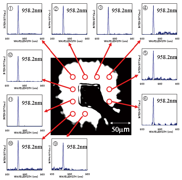
Fig 3. Near-field pattern with lasing spectra at various points of the device.
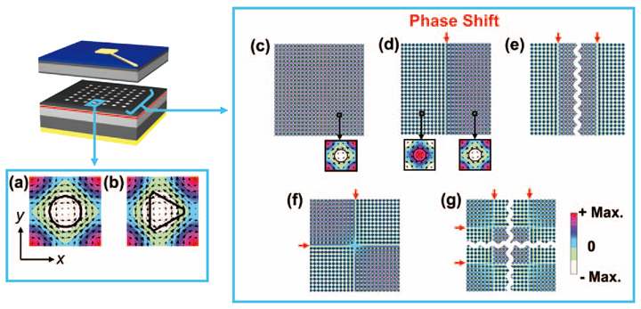
Fig. 4 Near-field pattern with lasing spectra at various points of the device. Electromagnetic field distribution in various photonic crystal lasers. Black arrows represent the electric field, and shading indicates the magnetic field in the direction perpendicular to the paper. Field distributions around the lattice points are shown for (a) circular lattice points and (b) triangular lattice points. Field distributions over the entire crystal are shown for circular lattice points with (c) no phase shift, (d) one phase shift in the x-direction, (e) two phase shifts in the x-direction, (f) one phase shift in both directions, and (g) two phase shifts in both directions. The phase in each region was shifted by across the boundary where the phase shift was introduced.
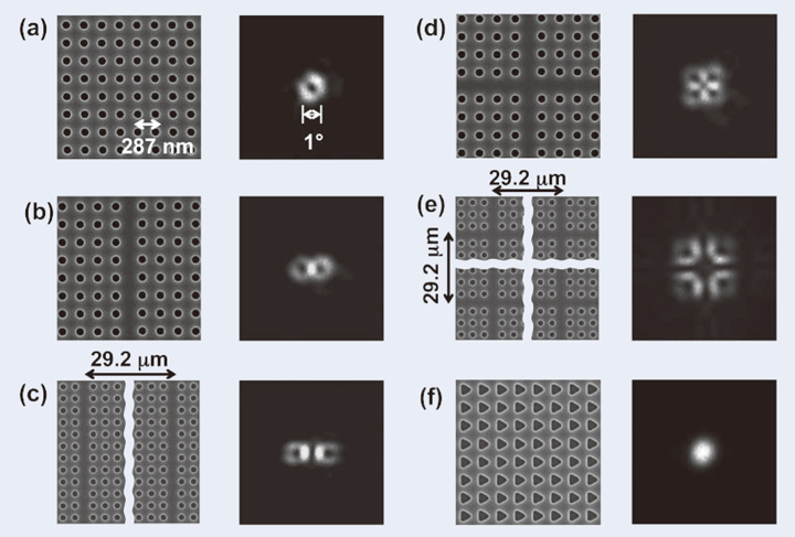
Fig. 5 Electron micrographs (left-hand panels) and obtained beam patterns (right-hand panels) of fabricated photonic crystals used to construct lasers. Photonic crystals with circular lattice points are shown with (a) no shift of the lattice period, (b) one lattice shift in one direction, (c) two lattice shifts in one direction, (d) one lattice shift in both directions, and (e) two lattice shifts in both directions. (f) Triangular lattice points with no phase shift.
Watt-class high-power, high-beamquality photonic-crystal lasers
In the previous section, the photonic crystal was embedded in the device by a wafer-bonding technique, where bonded interface may contain many defect states which absorb the lasing light and make it difficult to realize high power operation. To avoid such degradation of performance, we changed the method to introduce the photonic crystal into the device from a wafer bonding to a crystal growth technique such as organometallic vapor phase epitaxy (OMVPE) [10,11], and found that the air holes of photonic crystal can be retained even by the crystal growth technique. Figure 6 (a) shows the schematic of the device fabricated by two-step OMVPE. Note that the growth direction was downward. Figure 6 (b) shows a plan-view scanning electron microscope (SEM) image of the photonic crystal with right-isosceles-triangle-shaped air holes before the crystal growth. A typical crosssectional SEM image of a row of air holes embedded by OMVPE is shown in Fig. 6(c). It is clearly seen that the air holes were successfully embedded in the device, where the air holes become narrower towards the lower side of the device, whereas the upper parts of the air holes maintain an almost uniform shape with vertical side walls.
I then describe the lasing characteristics of the fabricated device [12] under the room-temperature (RT) continuous -wave (CW) condition . The corresponding experimental results are shown in Fig. 7(a) – (c). A maximum CW output power of 1.5 W at 2.5 A was achieved with a narrow, single-lobed beam of low divergence. When the output power was less than 0.5 W, the beam quality was quantitatively evaluated by measur ing the value of M2. For an ideal Gaussian beam, M2 is known to be unity, but it increases when the beam quality is degraded due to the transverse multimode. Measurements of M2 were performed under room-temperature CW conditions, and we found that M2 was kept almost at ~1.0 in both the x- and y-directions up to a power up to 0.5 W, indicating that a fundamental single transverse mode is maintained. Note that the beam divergence angle was less than 3° even at 1.5W power level.
Lasers with such a nar row beam divergence should enable unique applications that do not require any lens. We examined the direct irradiation of a sheet of paper placed 8.5 cm from the PCSEL to demonstrate such lens-f ree potential under CW operation at 25 °C. The light output was set to 0.86 W at a current of 1.7 A. The paper was burnt, forming a small hole immediately after radiation, as shown in Fig. 8. Although this is just a simple demonstration, it shows the potential of lens-free applications.
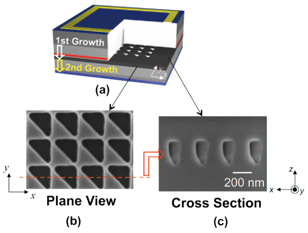
Fig. 6 (a) Schematic of the device fabricated by two-step OMVPE. (b) plan-view SEM image of the photonic crystal with right-isosceles-triangle-shaped air holes formed by electron beam lithography (JEOL JBX-6300FS) and dry etching. (c) A typical cross-sectional SEM image of a row of air holes embedded by OMVPE.
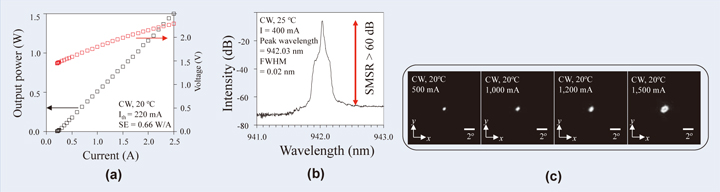
Fig. 7 Photograph taken immediately after direct radiation of the laser on a sheet of black paper placed 8.5 cm from the device.
Lasing characteristics of the device fabricated by two-step OMVPE. (a) I-L characteristics, (b) lasing spectra, and (c) farfield patterns at various current injection levels.
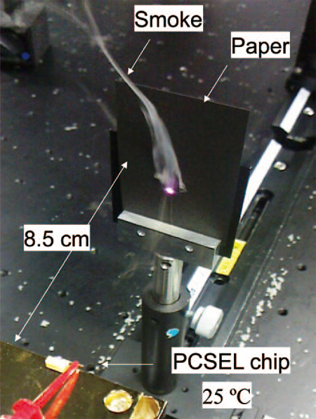
Fig. 8 Photograph taken immediately after direct radiation of the laser on a sheet of black paper placed 8.5 cm from the device.
Conclusion (or Summary)
I have described the current status and recent developments in the field of photonic-crystal lasers. It has been shown that the band-edge effect of twodimensional photonic crystals enables large-area single longitudinal and t ransver se mode lasing oscillation, as well as complete control over the beam patterns obtained. It has been also described that a device with an output power exceeding 1.5 watt under CW condition at RT. Our work represents an important milestone for innovation in the field of lasers because it provides a route towards overcoming limitations in applications that suffer from low beam quality, which opens the door to a wide range of applications in material processing, laser medicine, nonlinear optics, sensing and so on.
Acknowledgments
The author thanks members of Noda’s Lab., Kyoto University, and Rohm and Hamamatsu Photonics for the collaboration. This work was supported in part by JST, ACCEL & CREST, C-PhoST, MEXT, Japan.
References
[ 1 ] M. Imada, S. Noda, A. Chutinan, T. Tokuda, M. Murata, and G. Sasaki : "Coherent twodimensional lasing action in surface-emitting laser with triangular-lattice photonic crystal structure," Appl. Phys. Lett., vol.75, pp.316-318 (1999).
[ 2 ] S. Noda, M. Yokoyama, M. Imada, A. Chutinan, M. Mochizuki, “Polarization Mode Control of Two- Dimensional Photonic Crystal Laser by Unit Cell Structure Design,” Science, vol.293, pp. 1123-1125 (2001).
[ 3 ] M. Imada, A. Chut inan, S. Noda, and M. Mochi zuki , "Mult idi rect ional ly di st r ibuted feedback photonic crystal lasers", Physical Review B, Vol.65, No.19, pp.195306 (2002).
[ 4 ] K. Sakai, E. Miyai, T. Sakaguchi, D. Ohnishi, T. Okano, and S. Noda, "Lasing band edge identification for a surface-emitting photoniccrystal laser," IEEE Journal of Selected Area in Communications, vol.23, no.7, pp.1330-1334 (2005).
[ 5 ] D. Ohnishi, T. Okano, M. Imada, and S. Noda, “Room Temperature Continuous Wave Operationof a Surface-Emitting Two-Dimensional Photonic Crystal Diode Laser,” Optics Express, vol.12, pp.1562-1568 (2004).
[ 6 ] E. Miyai, K. Sakai, T. Okano, W, Kunishi, D. Ohnishi, and S. Noda, "Lasers producing tailored beams", Nature, Vol.441, No.7096, pp.946-946 (2006).
[ 7 ] H. Matsubara, S. Yoshimoto, H. Saito, Y. Jianglin, Y. Tanaka, and S. Noda, "GaN photonic-crystal surface-emitting laser at blue-violet wavelengths", Science, Vol. 319, No. 5862, pp. 445-447, (2008).
[ 8 ] Y. Kurosaka, S. Iwahashi, Y. Liang, K. Sakai, E. Miyai, W. Kunishi, D. Ohnishi, and S. Noda, "Onchip beam-steering photonic-crystal lasers", NATURE PHOTONICS, Vol.4, No. 7, pp. 447-450 (2010).
[ 9 ] Y. Liang, P. Chao, K. Sakai, S. Iwahashi, and S. Noda, "Three-dimensional coupled-wave model for square-lattice photonic crystal lasers with transverse electric polarization: A general approach", Physical Review B, vol. 84, no. 19, 195119 (2011).
[10] T. Sakaguchi, W. Kunishi, S. Arimura, K. Nagase,E. Miyai, D. Ohnishi, K. Sakai, S. Noda, “Surface- Emitting Photonic-Crystal Laser with 35W Peak Power,” The Conference on Lasers and Electro- Optics and the International Quantum Electronics Conference 2009, CTuH1 (2009).
[11] K. Hi rose, Y. Kurosaka, A. Watanabe, T. Sugiyama, Y. Liang, and S. Noda, “High power Photonic-Crystal Surface-Emitting Lasers,” The 10th Conference on Lasers and Electro-Optics Pacific Rim (CLEO-PR 2013), ThI1-4 (2013).
[12] M. Nishimoto, K. Ishizaki, K. Maekawa, K. Kitamura, and S. Noda, "Air-Hole Retained Growt h by Mol e c u l a r Be am Epi t a x y for Fabricating GaAs-Based Photonic-Crystal Lasers", Applied Physics Express, vol. 6, no. 4, 042002, (2013).
[13] K. Hirose, Y. Liang, Y. Kurosaka, A. Watanabe, T. Sugiyama, and S. Noda, “Watt-class high-power, high-beam-quality photonic-crystal lasers”, Nature Photonics, vol.8, pp.406-411 (2014).doi: 10.1038/ ncomms4138.