Elucidation of Deterioration Mechanism for Organic Solar Cells – Toward Highly Efficient Solar Cells –
JEOLnews Volume 49, Number 1, 2014
Kazuhiro Marumoto
University of Tsukuba
We report on an electron spin resonance (ESR) study of polymer solar cells to investigate accumulated charge carriers in these devices under device operation from a microscopic viewpoint. Light-induced ESR (LESR) signals and device characteristics were simultaneously measured using the same device under simulated solar irradiation. From the ESR analysis, the molecules where
photogenerated hole carriers were accumulated are clearly identified as poly(3-hexylthiophene) (P3HT). Moreover, the simultaneous measurements of ESR and device characteristics demonstrate a clear correlation between the increased LESR intensity and deteriorated device performance. The ESR study reveals that the deep trapping sites for photogenerated hole carriers are located at
interfaces between a hole buffer layer poly(3,4-ethylenedioxythiophene):poly(4-styrenesulfonate) (PEDOT:PSS) and an active layer P3HT:[6,6] -phenyl C61-butyric acid methyl ester (PCBM), which can be ascribed as the main mechanism for the reversible deterioration of the device performance of polymer solar cells.
Introduction
Organic thin-film solar cells are a promising alternative source of electrical energy because of their printable and flexible device structure, light weight, and low-cost production.[1-3] Solar cells have been investigated using a variety of methods with the aim of improving their performance.[4-10] There has been a significant amount of interest in the high power conversion efficiency (PCE) of more than 10% that was recently obtained in organic thin-film solar cells due to their potential practical applications.[11,12] In addition to device performance, the durability of solar cells is an important problem for the practical use of solar cells. For durability studies, degradation of solar cells due to extrinsic factors such as oxygen and water has been reported, where material s and device structures were irreversibly degraded. [13-15] Moreover, in addition to their reversible degradation, the reversible initial deterioration of device performance without material degradation has been reported for a polymer solar cell using methods that employ thermal stimulated current (TSC) and cur rent density (J ) -voltage (V) measurement s . [16,17] The studied polymer solar cell was a bulkheterojunction (BHJ) thin-film solar cell with blend films of a conducting polymer regioregular poly(3- hexylthiophene) (P3HT) and a soluble fullerene [6,6] -phenyl C61-butyric acid methyl ester (PCBM), which has been widely studied as a typical polymer solar cell.[1-10,16,17] The polymer solar cell has a device structure of indium-tin oxide (ITO)/poly(3,4- ethylenedioxythiophene):poly(4-styrenesulfonate) (PEDOT:PSS)/P3HT:PCBM/Al, where PEDOT:PSS is a typical hole buffer layer and has been widely used to improve device performance.[1-13,16,17] The previous studies reported that the device performance gradually deteriorated during device operation and that the deterioration could be recovered via thermal annealing.[16,17] In other words, the deterioration has been ascribed to an accumulation of photogenerated charge carriers during device operation rather than to the degradation of organic materials and/or device structures.[16,17] The TSC study indicated that the accumulation sites were located at interfaces between active layers and electrodes with various trapping levels.[16] However, a more detailed study clarifying molecules and these sites where charge carriers are accumulated (trapped) without molecular degradation has not yet been conducted, which will be extremely impor tant for fur ther device per formance and durability improvements.
Electron spin resonance (ESR) is one promising method for such a microscopic characterization of charge-accumulation sites because it is a highly sensitive and powerful approach that is capable of investigating organic materials at the molecular level. [18-21] This method has the advantage of being able to directly observe accumulated charge carriers without detrapping carriers via thermal stimulation, as used in 1-1-1 Tennodai, Tsukuba, Ibaraki 305-8573, Japan E-mail: marumoto@ims.tsukuba.ac.jp (2014) Vol. 49 No. 1 JEOL News 44 the TSC method. This ESR method has successfully clarified the microscopic properties of charge-carrier states in organic devices, including spin states and their spatial extent of wave function in pentacene,[18] fullerene (C6 0) , [19] and P3HT[19, 21] at device interfaces. The ESR method has also been applied to pentacene/C60 heterojunction organic thin-film solar cells and their organic layered films; these studies directly observed charge formation in pentacene layers during device fabrication under dark conditions.[22,23] However, the accumulation of photogenerated charge carriers in polymer solar cells under device operation has not yet been investigated using the ESR method. Such an investigation from a microscopic viewpoint would be useful in clarifying the accumulation sites, which would help to improve device durability and performance.
In this news, we report on an ESR study of P3HT:PCBM polymer solar cells to investigate accumulated charge carriers in these devices under device operation.[24] We measured light-induced ESR (LESR) signals and device characteristics (short-circuit current and open-circuit voltage) simultaneously using the same device under simulated solar irradiation. From the ESR analysis , the mole cules where photogenerated hole carriers were accumulated are clearly identified as P3HT. Moreover, the simultaneous measurements of ESR and device characteristics demonstrate a clear correlation between the increased LESR intensity and deteriorated device performance. With the use of organic layered films of PEDOT:PSS/ P3HT:PCBM, the ESR study reveals that the deep trapping sites for photogenerated hole carriers are located at PEDOT:PSS/P3HT:PCBM inter faces, which can be ascribed as the main mechanism for the reversible initial deter ioration of the device performance of polymer solar cells.
Experimental
Commercially available P3HT (Sigma-Aldrich, Plexcore OS 1100, regioregularity: 98.5%), PCBM (Frontier Carbon, nanom spectra E100, purity: 99.2%), and PEDOT:PSS (Clevios PAI4083) were used to fabricate the solar cells. The chemical structures of P3HT, PCBM, PEDOT, and PSS are provided in Fig. 1. The device structure was ITO/PEDOT:PSS (≈40 nm)/ P3HT:PCBM (≈160 nm)/Pd (1.2 nm)/LiF (0.6 nm)/Al (100 nm). PEDOT:PSS films were fabricated by spincoating an aqueous solution onto ITO-coated quartz substrates, followed by annealing at 140 °C for 10 min under an Ar atmosphere. Solutions of P3HT and PCBM (1:0.8 w/w) dissolved in o-dichlorobenzene (3.4 wt.%) were stirred with a magnetic stirrer for 30 min at 70 °C, and were spin coated on top of the PEDOT:PSS films at 1000 rpm for 75 s to form P3HT:PCBM films. The area of the interface between P3HT:PCBM and PEDOT:PSS was 3 mm × ≈14 mm. Then, Pd, LiF, and Al layers were deposited onto the P3HT:PCBM blend film to form the anode using a conventional vacuum sublimation technique under vacuum conditions below 2×10⁻⁴ Pa. Finally, the devices were annealed at 140 °C for 30 min under an Ar atmosphere and vacuum-sealed after wiring in an ESR sample tube. The device performance was confirmed to improve by the use of Pd on the anode side. We also obtained similar ESR results to those of the present study by using devices without Pd and LiF.
The J-V characteristics were evaluated using an Agilent Technology B1500A semiconductor device analyzer under simulated solar irradiation (AM 1.5G) with a 100 mW cm-2 intensity at 290 K under an Ar atmosphere. ESR measurements were performed using a JEOL RESONANCE JES-FA200 X-band spectrometer under vacuum conditions at 290 K. The number of spins, g factor, and linewidth of the ESR signal were calibrated using a standard Mn2+ marker sample. The absolute value of the number of spins was calculated using a solution (220 μl) of 4-hydroxy-2,2,6,6- tetramethylpiperidin-1-oxyl (TEMPOL) as a standard. The calibration of the g factor was performed by using a software program of the JEOL RESONANCE ESR system considering higher order correction to the effective resonance field. Its correctness was also confirmed by using 2,2-diphenyl-1-picrylhydrazyl (DPPH) as another standard sample. Simultaneous measurements of LESR and the device characteristics Jsc and Voc were performed using a Keithley 2612A source meter under simulated solar irradiation (AM 1.5G) with a 100 mW cm-2 intensity with a Bunkoukeiki OTENTOSUN-150BXM solar simulator at 290 K. The simultaneous measurements under the open-circuit condition were performed immediately after performing simultaneous measurements under the short-circuit condition using the same device.
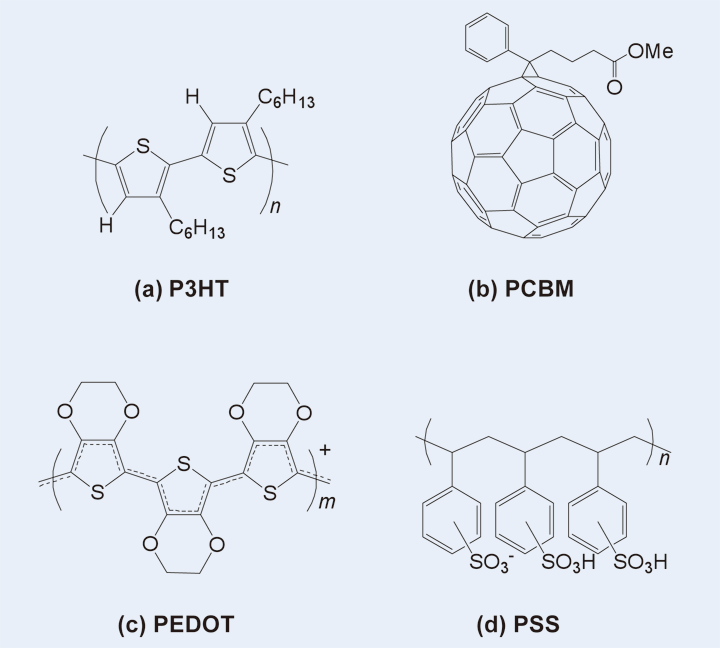
Fig. 1 Chemical structures of: a) regioregular poly(3-hexylthiophene) (P3HT), b) [6,6]-phenyl C61-butyric acid methyl ester (PCBM), c) poly(3,4-ethylenedioxythiophene) (PEDOT), and d) poly(4-styrenesulfonate) (PSS).
Results and Discussion
Firstly, we describe the device characteristics of our solar cells. When we fabricated solar cells with an active area of 2 mm × 2 mm using an ITO substrate with a conventional size of 20 mm × 20 mm, our devices had the following typical parameters: a short-circuit current density (Jsc) of ≈7.1 mA cm-2, an open-circuit voltage (Voc) of ≈0.66 V, a fill factor (FF) of ≈0.60, and a PCE of ≈2.8%. These values are equivalent to those reported by other groups.[3- 9,16,17] Thus, we have confirmed standard device operation using our device fabrication method. However, the device parameters of the cells for the ESR experiments deteriorated, compared with those of the above cells because of the following difficulties. Firstly, the use of a narrow ITO substrate with a size of 3 mm × 20 mm (see Fig. 1c of Ref. 22) was necessary because we needed to insert the device into an ESR sample tube with an inner diameter of 3.5 mm. Secondly, to overcome the low signal-tonoise (SN) ratio of the LESR signal due to device operation, we needed to fabricate a device with a large active area; we adopted an active area of 2 mm × 10 mm in this study. Thus, the film quality of the asymmetric active area deteriorated because of the variation in film thickness, which was caused by the difficulties of spin coating using the narrow ITO substrate. As a result, the device characteristics deteriorated; Jsc and Voc decreased to approximately 2.2 mA cm-2 and 0.35 V, respectively. Despite this decreased device performance, our devices for the ESR experiments exhibited similar performance deterioration under device operation as that reported by other groups . [16,17] Therefore, the present microscopic character ization by ESR analysis is considered to be useful for clarifying the essential problems of performance deterioration under device operation, as demonstrated below.
Next, we present the light-induced ESR (LESR) signals of the devices under device operation. Figure 2 demonstrates the dependences of the LESR signals of the same device on the duration of simulated solar irradiation under: a) short-circuit condition, and b) open-circuit condition. Here, the LESR signals were obtained by subtracting the ESR signal under dark conditions from that under simulated solar irradiation. The vertical axis is plotted using a unit of peak-to-peak ESR intensity of the ESR signal for a standard Mn2+ marker sample, IMn, which is attached to the inside wall of the ESR cavity of the JEOL RESONANCE ESR system. In our experiment, we used a continuous-wave method with a modulation frequency of 100 kHz for the external magnetic field. Thus, the photogenerated charge carriers with short lifetimes less than 10 μs cannot be observed using the present ESR method. Freely diffusive charge carriers to electrodes contribute the standard operation of the device. Therefore, the observed LESR signals are due to the accumulation of photogenerated charge carriers with lifetimes longer than 10 μs, namely, trapped photogenerated carriers. As revealed in Fig. 2a,b, gradual increases in the LESR intensities are clearly observed under both operation conditions. The increased rate of the LESR signal under the short-circuit condition is larger than that under the open-circuit condition. The g factor and peak-topeak ESR linewidth, Hpp, are determined to be: a) g = 2.0022 and Hpp = 0.25 mT, and b) g = 2.0023 and Hpp = 0.24 mT. These values are consistent with those of hole carriers (positive polarons) in P3HT films in organic field-effect devices.[19,21] Therefore, the LESR observation directly demonstrates that the observed spin species are photogenerated hole carriers accumulated in P3HT molecules.
To clarify the locations of accumulated holes fur ther, we per formed LESR measurement s for organic layered films of ITO/P3HT:PCBM, ITO/ PEDOT:PSS, and ITO/PEDOT:PSS/P3HT:PCBM. For the ITO/P3HT:PCBM and ITO/PEDOT:PSS/ P3HT:PCBM films, we observed the same LESR signal as that observed in Fig. 2a,b. However, for the ITO/PEDOT:PSS films, we did not observe such a LESR signal. Moreover, the ESR signal of PCBM has been reported to have g-tensor values of 1.9982 - 2.00058, [25-27] which differ radically from that observed in Fig. 2a,b. Furthermore, the ESR signals of PEDOT:PSS and PEDOT have been reported to exhibit a broader ESR linewidth than that observed in Fig. 2a,b. [28,29] Therefore, we can ascribe the LESR signals observed in Fig. 2a,b to accumulated hole carriers in P3HT. We here comment that the reason for the absence of LESR signal from radial anion (electron) on PCBM is ascribed to the rapid spin relaxat ion of ful lerene’s elect ron at room temperature.[19,27]
Next, we present the results of simultaneous measurements of LESR and device characteristics using the same device. To present the ESR results, we use the number of spins , Nspin , due to the accumulation of photogenerated hole carriers in P3HT varied from that before irradiation at each experiment, which was obtained by integrating the LESR signal twice at approximately 320.5-322 mT and comparing this value with the standard Mn2+ marker sample. Fig. 2c,d illustrate the dependences of Nspin and the device parameters Jsc and Voc on the duration of the simulated solar i r radiation, respectively. These results indicate that an increase in Nspin clearly correlates with the deterioration of the device performance. That is, Nspin monotonically increases and Jsc and Voc concomitantly decrease as the duration of simulated solar irradiation increases. This clear correlation demonstrates that the accumulation of photogenerated hole carriers in P3HT deteriorates the device parameters Jsc and Voc. To the best of our knowledge, this is the first instance in which such a clear correlation between the microscopic ESR characteristics and macroscopic device parameters has been observed. The charge accumulation affects an internal electric field in the device, which prevents current flow and creates additional potential in the cells, as disscussed later.
The influence of the increased charge accumulation (carrier density) on Jsc and Voc were investigated in detail by other groups. [16,17] The studies showed the decreases in Jsc and Voc during device operation, which are consistent with those of our device. Note that the reversibility of the charge accumulation and the device parameters Jsc and Voc was confirmed from ESR and J-V characteristics after irradiation off, which is consistent with that of the previous works.[16,17] We comment that the longlived accumulated charge carriers in polymer films have been reported by several groups, which were caused by deep trappings due to low temperatures[30] or extrinsic factors such as oxygen under irradiation. [27] The inf luence of traps due to such extrinsic factors on Jsc and Voc have been also studied.[13,14] The inf luence is an interest ing problem for the present results because our device is vacuum sealed in an ESR sample tube, which is beyond the present research scope and is open for further study.
Next, we discuss the accumulation sites of the photogenerated hole carriers in more detail. As presented in Fig. 2c,d, the accumulation rate of the photogenerated hole carriers under the shortcircuit condition is larger than that under the opencircuit condition. Under the short-circuit condition, an internal electric field exists in the BHJ active layer in the device, which causes the migration of photogenerated hole carriers to ITO electrodes through the inter face between the PEDOT:PSS and P3HT:PCBM layers. Thus, one can consider that the di f ference for the ac cumulat ion rates between the short- and open- circuit conditions can be ascribed to the effect of the PEDOT:PSS/ P3HT:PCBM inter faces. To clarify the effect of the PEDOT:PSS/P3HT:PCBM interfaces on hole accumulation, we examined the transient response of LESR for layered thin films of ITO/P3HT:PCBM and ITO/PEDOT:PSS/P3HT:PCBM upon simulated solar irradiation. Figure 3a,b present the transient responses of Nspin for: a) ITO/P3HT:PCBM, and b) ITO/ PEDOT: PSS / P 3HT: PCBM. For ITO/ P3HT:PCBM, Nspin monotonically increases under simulated solar irradiation. When irradiation ceases, Nspin sharply decreases to a small value, and then, the small remaining component gradually decreases ( see Fig. 3a) . However, for ITO/PEDOT:PSS / P3HT:PCBM, a different behavior was observed compared with that of ITO/P3HT:PCBM. That is, a large remaining component was clearly observed after turning off the irradiation (see Fig. 3b). The lifetime of the remaining component is extremely long, more than 40 h, even at room temperature. Therefore, this result demonstrates that PEDOT:PSS insertion between ITO and P3HT:PCBM causes the hole accumulation sites with deep trapping levels in P3HT at PEDOT:PSS/P3HT:PCBM interfaces. Using this hole accumulation, the different rates of increase for Nspin observed in Fig. 2 can be reasonably explained because hole carriers are easily accumulated at the PEDOT:PSS/P3HT:PCBM inter faces due to the flow of short-circuit currents. We here comment on the sharply increasing and decreasing components upon irradiation on and off, respectively, in Fig. 2c,d, and 3a,b. These LESR signals are due to shallowly t rapped photogenerated holes in P3HT, which accumulation sites are probably located at bulk materials.
The findings from the ESR study are summarized in Fig. 3c, which helps to explain the hole accumulation at the interfaces under simulated solar irradiation. Firstly, the hole accumulation sites with deep trapping levels are formed by depositing P3HT:PCBM films on a PEDOT:PSS layer (see lefthand side in Fig. 3c). Secondly, photogenerated hole carriers are accumulated at deep trapping sites in P3HT molecules at the PEDOT:PSS/P3HT:PCBM interfaces (see the right-hand side of Fig. 3c). This hole accumulation is enhanced by the current flow at the interfaces because of the internal electric field under the short-circuit condition. We here explain an energy-level shift in the highest occupied molecular orbital (HOMO) of P3HT at the interfaces shown in Fig. 3c. This energy-level shift is related to the interfacial electric dipole layer, which can be caused by an elect ron t ransfer f rom P3HT to PEDOT because of the energy difference between the HOMO of P3HT (4.7-5.1 eV)[31,32] and the work function of PEDOT:PSS (5.3 eV).[8,22] This electron transfer forms holes in P3HT under the dark condition, as discussed in a previous ESR study on pentacene/C60 heterojunction solar cells with PEDOT:PSS holebuffer layers.[22] We confirmed this additional hole formation in the present study by measuring ESR signal s of layered f i lms of quar tz /P3HT:PCBM and quartz /PEDOT:PSS/P3HT:PCBM under dark conditions before simulated solar irradiation. That is, the number of spins of P3HT under dark conditions for quartz/PEDOT:PSS/P3HT:PCBM was measured to be 3.2×10¹², which is larger than that of 4.6×10¹¹ for quartz/P3HT:PCBM. This result demonstrates the additional hole formation in P3HT due to the electron transfer f rom P3HT to PEDOT:PSS under dark conditions. Note that this hole formation under dark conditions is not presented in Fig. 3c to present the hole accumulation in P3HT clearly under simulated solar irradiation mentioned above.
In the fol lowing, we discuss the cor relation shown in Fig. 2c,d in more detail. Firstly, we explain the decrease in Voc using an interfacial electric dipole layer due to accumulated holes at the PEDOT:PSS/ P3HT:PCBM interfaces. When an interfacial electric dipole layer due to accumulated charges is formed, a vacuum-level shift occurs at the inter face. [33] Such vacuum-level shift decreases Voc of solar cells because of the energy-level shift for molecules at the interface.[34] We here evaluate the interfacial electric dipole length (d) due to the hole accumulation at PEDOT:PSS /P3HT:PCBM inter fac e us ing the capacitance formula Q = CV. Let S be the area at the interfaces, Nspin and Voc be the increase in Nspin and the decrease in Voc due to the hole accumulation at the interfaces, respectively, e be the elemental charge, 0 be the permittivity in vacuum, r be the dielectric constants of P3HT:PCBM materials,[35] then, d may be expressed as follows:
Using the experimental values of S = 0.4cm2 , Nspin = 1.2×10¹², and Voc = 0.11 V, d is evaluated to be approximately 1 nm. This length probably corresponds to the length of alkyl-side chains in P3HT; [36] the alkyl- side chains are insulator s without electrons. It should be noted that Voc is proportional to Nspin, which well explains the experimental result shown in Fig. 2d.
Next, we explain the decrease in Jsc using chargecarrier scattering due to the hole accumulation. Such scattering is considered to be independent of other charge-carrier scattering mechanisms in solar cells, and then we may use the Matthiessen’s rule for the mobility μ in the cells as follows:[37]
Here, we use two mobility constituents, μSC and μHA, related to the charge-carrier scattering in solar cells without and with the hole accumulation, respectively. The latter depends on Nspin with a proportionality constant c. Using Equation (2), we may express the current density j in solar cells using charge density n and internal electric filed E in the cells as follows:

Equation (3) shows that j decreases as Nspin increases. This behavior well explains the experimental result shown in Fig. 2c. Therefore, the charge- car r ier scattering induced by the accumulated holes in the cells decreases Jsc during device operation under simulated solar irradiation.
Finally, we comment on the disordered molecular or ientation for the hole-accumulation sites. Figure 4 shows the ESR and LESR signals of P3HT in an organic layered thin film of ITO/ PEDOT:PSS/P3HT:PCBM under dark condition and simulated solar irradiation, respectively. These signals were obtained by subtracting the ESR signal of PEDOT:PSS from that of ITO/PEDOT:PSS/ P3HT:PCBM to present the ESR signal of P3HT clearly. Under dark condition, the ESR signal of P3HT was observed, which can be ascribed to the hole formation due to the charge transfer between P3HT and PEDOT:PSS, as mentioned above. [22] The obtained g value of 2.0018 means that the holeformation sites are attributable to P3HT molecules in ordered lamella structures from the anisotropy of the g values for P3HT molecules.[21] However, the LESR signal of P3HT after simulated solar irradiation shows the different g value of 2.0022 from that for ordered P3HT molecules. This finding clearly demonstrates t hat t he mole cu l a r or ient at ion for t he hole - accumulation sites is disordered and is different from that in the ordered lamella structures. Note that the disordered molecular orientation is further confirmed by the detailed anisotropy for the LESR signal.
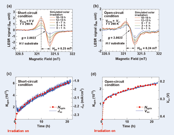
Fig. 2 a,b) LESR signals of ITO/PEDOT:PSS/P3HT:PCBM/Pd/LiF/Al at approximately 320.4-322 mT for various exposure times to simulated solar light (AM 1.5G) with a 100 mW cm-2 intensity at 290 K under short-circuit condition (a) and open-circuit condition (b), respectively. The external magnetic field H is parallel to the substrate. The vertical axis is plotted using a unit of peak-to-peak ESR intensity of the ESR signal of a standard Mn2+ marker sample, IMn. The data were obtained by averaging LESR signals measured under irradiation during 1 h. c,d) The dependences of Nspin and the device parameters Jsc
(c) and Voc (d) on the duration of simulated solar irradiation at 290 K, respectively. The Nspin is obtained from the averaged LESR signal of P3HT under irradiation for 1 h, and is plotted at each averaged time over 1 h.
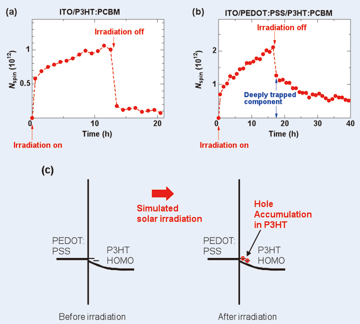
Fig. 3 Transient responses of Nspin for organic layered thin films of: a) ITO/P3HT:PCBM, and b) ITO/PEDOT:PSS/P3HT:PCBM upon simulated solar irradiation at 290 K. The Nspin is obtained from the averaged LESR signal of P3HT under irradiation for 1 h at 290 K, and is plotted at each averaged time over 1 h. c) Energy diagrams at the PEDOT:PSS/P3HT interfaces, which schematically explain the accumulation of photogenerated hole carriers in P3HT molecular sites after simulated solar irradiation.
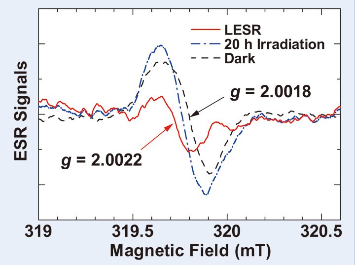
Fig. 4 The ESR and LESR signals of P3HT in ITO/PEDOT:PSS/P3HT:PCBM under dark condition and simulated solar irradiation at 290 K, respectively. The external magnetic field is parallel to the substrate. Dashed line shows the ESR signal under dark condition. Dashed-dotted line shows the ESR signal after 20 h simulated solar irradiation. Solid line shows the LESR signal, which is obtained by subtracting the ESR signal under dark conditions from that under simulated solar irradiation.
Conclusion
We have fabr icated polymer solar cell s of ITO/PEDOT:PSS /P3HT:PCBM/Pd /LiF/Al and performed simultaneous measurements of LESR and device characteristics under simulated solar irradiation to clarify the deterioration mechanism Fig. 4 The ESR and LESR signals of P3HT in ITO/PEDOT:PSS/P3HT:PCBM under dark condition and simulated solar irradiation at of device performance during device operation at the molecular level. We observed a monotonic increase in LESR signals under simulated solar irradiation, which is ascribed to the accumulation of photogenerated hole carriers in P3HT of the device under operating condition from the microscopic viewpoint for the first time. We also observed a clear correlation between the increase in Nspin due to the hole accumulation and the deterioration of the device parameters Jsc and Voc. This correlation demonstrates that the hole accumulation in P3HT causes the initial deterioration of the device performance. The sites of hole accumulation with deep trapping levels were identified as being formed in P3HT at the PEDOT:PSS/P3HT:PCBM interfaces from the study of organic layered films, which explains the more rapidly increasing rate of LESR for the devices under the short-circuit condition than under the open-circuit condition. Thus, modifications at the PEDOT:PSS/ P3HT:PCBM interfaces are recommended to improve device durability by preventing hole accumulation under device operation. For other solar cells, we also propose improvements in device durability by reducing the charge accumulation in the cells during device operation based on the microscopic information obtained from this and future ESR studies.
Acknowledgments
The author thanks T. Nagamori and M. Yabusaki for their collaboration. This research was partly supported by Grants-in-Aid for Scientific Research (24560004 and 22340080) from the Japan Society for the Promotion of Science (JSPS) and by JST, PRESTO.
References
[ 1 ] C. J. Brabec, Sol. Energy Mater. Sol. Cells, 83, 273 (2004).
[ 2 ] P. Kopola, T. Aernouts, R. Sliz, S. Guillerez, M. Ylikunnari, D. Cheyns, M. Valimaki, M. Tuomikoski, J. Hast, G. Jabbour, R. Myllylä , A. Maaninen, Sol. Energy Mater. Sol. Cells, 95, 1344 (2011).
[ 3 ] M. Kaltenbrunner, M. S. White, E. D. Głowacki, T. Sekitani, T. Someya, N. S. Sariciftci, S. Bauer, Nat. Commun. 3, 770 (2012).
[ 4 ] G. Li, V. Shrotriya, J. Huang, Y. Yao, T. Moriarty, K. Emery, Y. Yang, Nat. Mater. 4, 864 (2005).
[ 5 ] W. Ma, C. Yang, X. Gong, K. Lee, A. J. Heeger, Adv. Funct. Mater. 15, 1617 (2005).
[ 6 ] S. Günes, H. Neugebauer, N. S. Sariciftci, Chem. Rev. 107, 1324 (2007).
[ 7 ] E. Ahlswede, J. Hanisch, M. Powalla, Appl. Phys. Lett. 90, 163504 (2007).
[ 8 ] Y. Kim, A. M. Ballantyne, J. Nelson, D. D. C. Bradley, Org. Electron. 10, 205 (2009).
[ 9 ] G. Dennler, M. C. Scharber, C. J. Brabec, Adv. Mater. 21, 1323 (2009).
[10] J. S. Kim, J. H. Lee, J. H. Park, C. Shim, M. Sim, K. Cho, Adv. Funct. Mater. 21, 480 (2011).
[11] R. F. Service, Science 332, 293 (2011).
[12] M. A. Green, K. Emery, Y. Hishikawa, W. Warta, E. D. Dunlop, Prog. Photovoltaics: Res. Appl. 21, 1 (2013).
[13] M. Jørgensen, K. Norrman, F. C. Krebs, Sol . Energy Mater. Sol. Cells, 92, 686 (2008).
[14] A. Seemann, T. Sauermann, C. Lungenschmied, O. Armbruster, S. Bauer, H.-J. Egelhaaf, J. Hauch, Sol. Energy, 85, 1238 (2011).
[15] V. Singh, S. Arora, P. K. Bhatnagar, M. Arora, R. P. Tandon, J. Polym. Res. 19, 9899 (2012).
[16] K. Kawano, C. Adachi, Adv. Funct. Mater. 19, 3934 (2009).
[17] T. Yamanar i, H. Ogo, T. Taima, J. Sakai, J. Tsukamoto, Y. Yoshida, in 2010 35th IEEE Photovoltaic Specialist Conf. (PVSC), IEEE, p.001628 (2010).
[18] K. Marumoto, S. Kuroda, T. Takenobu, Y. Iwasa, Phys. Rev. Lett. 97, 256603 (2006).
[19] K. Marumoto, T. Sakamoto, S. Watanabe, H. Ito, S. Kuroda, Jpn. J. Appl. Phys. 46, L1191 (2007).
[20] K. Marumoto, M. Kato, H. Kondo, S. Kuroda, N. C. Greenham, R. H. Friend, Y. Shimoi, S. Abe, Phys. Rev. B 79, 245204 (2009).
[21] S. Watanabe, H. Tanaka, S. Kuroda, A. Toda, S. Nagano, T. Seki, A. Kimoto, J. Abe, Appl. Phys. Lett. 96, 173302 (2010).
[22] K. Marumoto, T. Fujimori, M. Ito, T. Mori, Adv. Energy Mater. 2, 591 (2012).
[23] M. Ito, K. Marumoto, Chem. Lett. 41, 696 (2012).
[24] T. Nagamori, K. Marumoto, Adv. Mater. 25, 2362 (2013).
[25] J. De Ceuster, E. Goovaerts, A. Bouwen, J. C. Hummelen, V. Dyakonov, Phys. Rev. B 64, 195206 (2001).
[26] O. G. Poluektov, S. Filippone, N. Martín, A. Sperlich, C. Deibel, V. Dyakonov, J. Phys. Chem. B 114, 14426 (2010).
[27] A. Aguirre, S. C. J. Meskers, R. A. J. Janssen, H.-J. Egelhaaf, Org. Electron. 12, 1657 (2011).
[28] J. Ouyanga, Q. Xu, C.-W. Chu, Y. Yang, G. Li, J. Shinar, Polymer 45, 8443 (2004).
[29] R. Jalili, J. M. Razal, P. C. Innis, G. G. Wallace, Adv. Funct. Mater. 21, 3363 (2011).
[30] N. A. Schultz, M. C. Scharber, C. J. Brabec, N. S. Sariciftci, Phys. Rev. B 64, 245210 (2001).
[31] M. C. Sch
お問い合わせ
日本電子では、お客様に安心して製品をお使い頂くために、
様々なサポート体制でお客様をバックアップしております。お気軽にお問い合わせください。