集束イオンビーム加工
集束イオンビーム加工
focused ion-beam milling, FIB
[目次:試料等(試料および試料作製)]
加速したガリウム(Ga)イオンを試料に集束して照射し、試料を削り取る加工法。バルク試料から透過電子顕微鏡観察用試料を作る過程においては、SEM観察しながら試料の位置をピンポイントで特定して薄片化することができる。特に、半導体デバイスの故障解析などでは欠かせない技術となっている。
まず、薄片化してTEM観察用試料とする部分が削られないように、FIB装置内で目的とする領域に白金あるいはカーボンの保護膜を形成する(図(a))。次に、高加速(30 kV程度)のGaイオンビームで目的の領域を厚さ数µm以下の試料片に加工する (図(b))。その試料片を取り出し、TEMグリッドに固定する (図(c))。最後に、試料の損傷が少ない低加速(5 kV程度)のGaイオンビームを用いて、10~100nm以下の薄片にする(図(d))。試料表面の損傷層(Gaイオン照射によるダメージ層)が問題になる場合は、さらに低加速(3kV以下)のGaイオンビームまたはアルゴンイオンビームを用いて損傷部分を取り除く。
図 (a)~(e)⇒図
図 (a)目的の場所を保護するためにカーボンや白金を薄膜蒸着する。(b)目的の場所の周囲をGaイオン照射によって削り、厚さ数µm以下の試料薄片を作製する。(c)試料薄片をTEMグリットに固定する。(d)目的の場所を厚さ10~100nm以下に薄片化する。(e)FIBにより薄膜化された試料をTEM観察する。
"Focused Ion Beam (FIB) milling" is a technique of a TEM specimen preparation to mill a bulk specimen with focused gallium (Ga) ions. The target region of the bulk specimen can be selectively thinned down to a desired shape while monitoring and controlling by SEM observation of the milling region. This technique is particularly indispensible for failure analysis of semiconductor devices.
The FIB milling procedure is as follows: First, the surface of the target region is coated with a platinum- or carbon-protective film in the FIB system to avoid the milling of the target region (Fig. (a)). Next, the target region is milled with a Ga ion beam of a high accelerating voltage of about 30 kV to prepare a section of a thickness of a few μm or less (Fig. (b)). Then, the prepared section is picked up from the bulk specimen and fixed onto a TEM specimen grid (Fig. (c)). Finally, the fixed specimen is milled with a Ga ion beam of a low accelerating voltage of about 5 kV (for decreasing damages to the specimen) to create a thin section of a thickness of 10 to 100 nm (Fig. (d)). If the damaged layers due to the irradiation of Ga ions remain, the layers are removed by another milling with a Ga ion beam of a lower accelerating voltage (about 3 kV or less) or with an argon (Ar) ion beam.
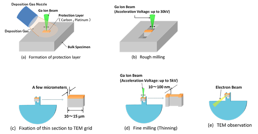
Fig. (a) Protection layer is formed on the target region by coating of carbon or platinum. (b) Surroundings of the target region are roughly milled with Ga ion beam to prepare a section (thickness: a few μm or less). (c) A section is fixed onto a TEM grid. (d) Thin section (thickness: 10 to 100 nm) is created from the target region by fine milling. (e) The thinned section prepared by FIB is subjected to TEM observation.
関連用語から探す
説明に「集束イオンビーム加工」が含まれている用語


