4D-STEM
4D-STEM
4 dimensional-scanning transmission electron microscopy
[目次:理論(電子の散乱/回折/結像)]
走査透過電子顕微鏡法(STEM)で2次元検出器(ピクセル型STEM検出器)を用いて回折図形のデータを取得し、4次元のデータを作成し、回折図形から得られる情報を反映させた電顕像を得る方法。
すなわち、電子プローブを試料上で2次元的に走査し、それと同期して2次元検出器で、試料の位置ごとの電子回折図形を記録する(図1a)。取得したデータは、試料の2次元位置データ(x, y)と、各位置に対応するカメラ上の2次元回折データ(u, v)から構成される4次元のデータキューブとなる(図1b)。この4次元データキューブから、特定の2次元位置(x, y) での2次元回折データ(u, v)の違いを利用して結晶相や結晶方位の分布や、試料中の磁場や電場の方向を可視化できる。また、これまでのSTEM法では十分に活用されていなかった回折図形の角度に依存した強度を利用して結晶構造の位置変化を可視化できる。 図2に回折図形を撮るときの収束角の違いを示す。図2bでは、隣り合う回折ディスクが重なっている。重なり部分からは回折波の位相が得られる。この位相を利用して試料の構造を精密化しているのがタイコグラフィーである。これらを総称して4D-STEM法と言う。
以下に、4D-STEM法を用いた3つの解析事例を示す。それぞれ、電子線の収束角と結像倍率(カメラ長)が異なり(図2)、それらは目的に応じて決められる。
結晶試料の方位解析の例(図3)
タイコグラフィーによる結晶構造の再生 (位相再生)の例 (図4)
試料中の磁場分布の可視化の例(図5)
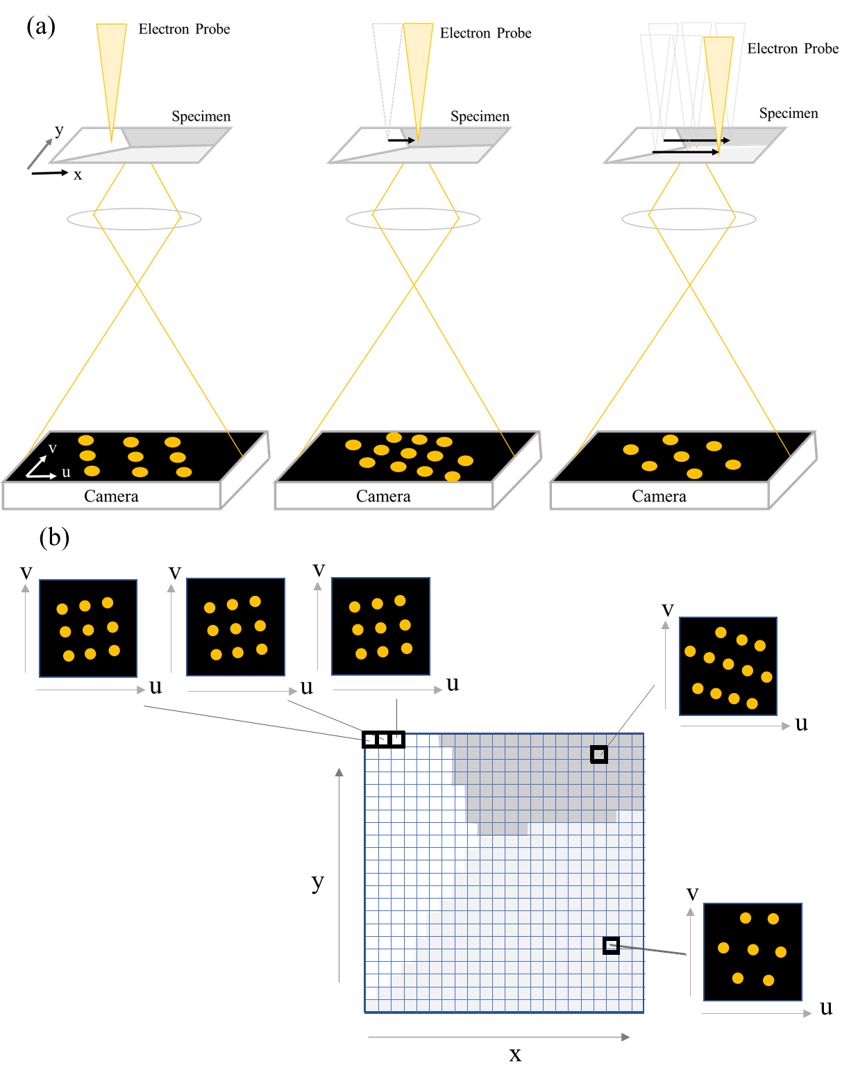
図1. (a) 4D-STEMデータの取得法:入射電子線を試料上で2次元的に走査して、各位置で2次元の電子回折図形をCCDまたはCMOSカメラで記録する。 (b) 4D-STEM法で取得した4次元のデータキューブの模式図。
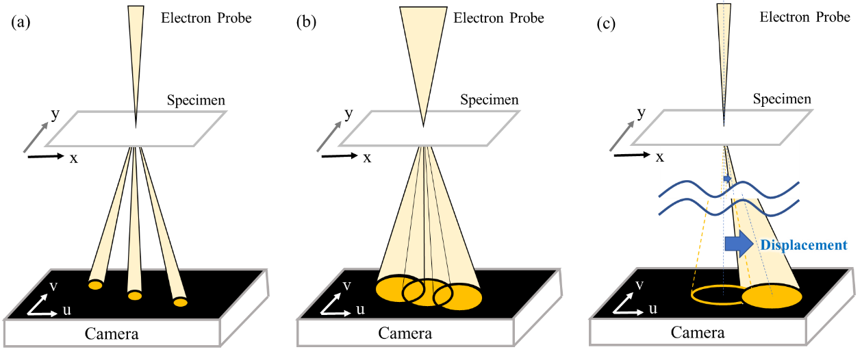
図2. 4D-STEMデータの取得条件の例。(a)収束角が小さい場合、(b)収束角が大きい場合、(c)カメラ長を長くして透過波および回折波ディスクの位置の変化を拡大する場合。
1. 結晶試料の方位解析の例
図3にMn-Znフェライト軟磁性材料から4D-STEMデータを取得し、粒界三重点近傍での結晶粒の方位解析を行った例を示す。図2aに示すように電子回折図形の透過ディスクと回折ディスクが分離するよう、収束角を小さくした状態(詳細は、TEM用語集のナノビーム回折の項参照)で4D-STEMデータを取得している。
取得した4次元データから、上段 (図3a) に示した試料の位置A, B, C, Dの4点での電子回折図形を抽出した。STEM ADF像(左図)上に示した点A, B, Dでは結晶の方位が異なること、中央の点Cでは非晶質になっていることが電子回折図形(右図)から分かった。このことから三つの粒界が交わる付近C(三重点と呼ぶ)では非晶質相が形成されていることが明らかになった。
さらに下段(図3b)に示すように、回折図形上で特定の回折斑点を選択して像モードにすれば、特定の方位に対応する画像を表示することができる。すなわち、結晶相由来の回折斑点(B、D)を選択すると、B、Dの方位に対応する結晶粒が可視化された。他方、回折斑点でない散漫散乱の領域Cを選択すると非晶質相が可視化された。
4D-STEMでは、従来の方法と異なり、取得した4次元のデータキューブから任意の位置での結晶方位を示すことができる。
2. タイコグラフィーによる結晶構造像の再生 (位相再生)の例
図4に高速高感度カメラを用いて4次元データを取得し、タイコグラフィー法を用いて試料の構造(位相)再生を行った例を示す。4D-STEMデータは、図2(b)に示すように、透過波ディスクと回折波ディスクが重なるように大きな収束角で取得した。
図4aは、取得した4次元データのうちの2次元空間成分に対応する像に対してフーリエ変換して得られた回折図形から抽出した指数3030と3030の収束電子回折ディスである。二つの回折ディスクは透過ディスクと重なっている。この重なり部分から回折波の振幅と位相が分かる。図4bに、回折波の位相を色で振幅を色の濃さで表した。回折ディスク3030と透過ディスク0000の重なり部分は青色で示した。回折ディスク3030と透過ディスクの重なり部分は赤色で示した。二つの領域では位相がπだけずれていることを表している。なお、黒破線で囲った領域AとBの外(黄緑色で示した部分)の強度は、ノイズ成分であるため振幅をゼロとする。図4cは、多くの反射に対して得られた振幅と位相を用いて再構成(逆フーリエ変換)した試料の結晶構造像(位相像)である。このような方法をタイコグラフィーという(TEM用語集のタイコグラフィーの項参照)。再生した構造像(位相像)ではSiの原子位置のみならず、Nの原子位置も高いコントラストで可視化できている。
3. 磁性材料中の磁区の可視化の例
図5は、4次元データを用いて磁性材料中の磁区を可視化した例。この場合には、回折データとして透過ディスクの磁化による偏向の方向が利用される(図2(c))。その際、偏向の方向と大きさを容易に検出できるように、結像系でカメラ長を長くし電子線の偏向成分を拡大して透過ディスクを撮影した。
4次元データとして記録された各位置での透過波の強度から、試料の像すなわちSTEM明視野像(図5(a))が再生される。4次元データから試料位置に対応する全画素について偏向成分(ここでは透過ディスクの相対的なズレの方向)を抽出することで、磁区構造が可視化されている(図(5b)) *。図5(b)中に示す矢印は、ズレの方向から決定した磁化の方向を示す。加えて、微分位相コントラストイメージング法によって得られた磁化の方向と有効な磁化の大きさを、それぞれ色の違いと色の濃さの違いで示した(左下のカラーホイール参照)。図5(b)の右には、4次元データから抽出した試料の3点からの透過ディスク示す。3点での磁化の方向の違いのために、それぞれの透過ディスクが、異なる方向にズレていることがわかる(ズレを見やすくするために赤色の補助十字線を書き入れた)。
なお、この試料は軟磁性材料であるため、磁区が安定するように還流磁区構造(磁化が全体として閉じている)を形成していることが分かる。
*参考までに微分位相コントラストイメージングの項も参照のこと。
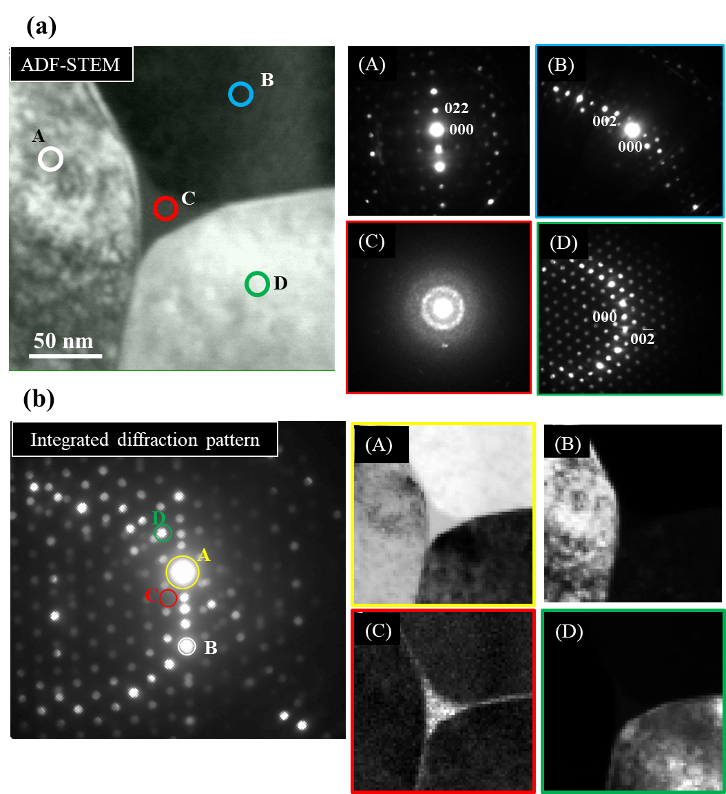
図3. 4D-STEM法で取得したMn-Znフェライト軟磁性材料の4次元データから三つの粒界が交わる近傍の結晶方位を解析した例。
上段(a) 左図はSTEM ADF像。右図は4次元のデータキューブからADF像の点A-Dから抽出した回折図形。
下段(b) 左図は試料全体にわたって積算した回折図形。右図は、左図の回折点A-Dを用いて再生したSTEM明視野像(A)とSTEM暗視野像(B-D)。
(これらのデータは奈良先端科学技術大学院大学 赤瀬善太郎特任准教授との共同研究による)

図4. 4次元データを用いたタイコグラフィー法による結晶構造(位相像)再生の例。試料は、β-Si3N4 [0001]入射。球面収差補正装置を用いて加速電圧200kV でデータを取得した。(a)得られ4次元データのうち、2次元空間成分に対応する像に対してフーリエ変換して得られた回折図形から抽出した指数3030と指数3030の収束電子回折図形。(b)青色と赤色は二つの領域で位相が反転していることを示す。 (c)タイコグラフィー処理により再生した結晶構造像(位相像)。
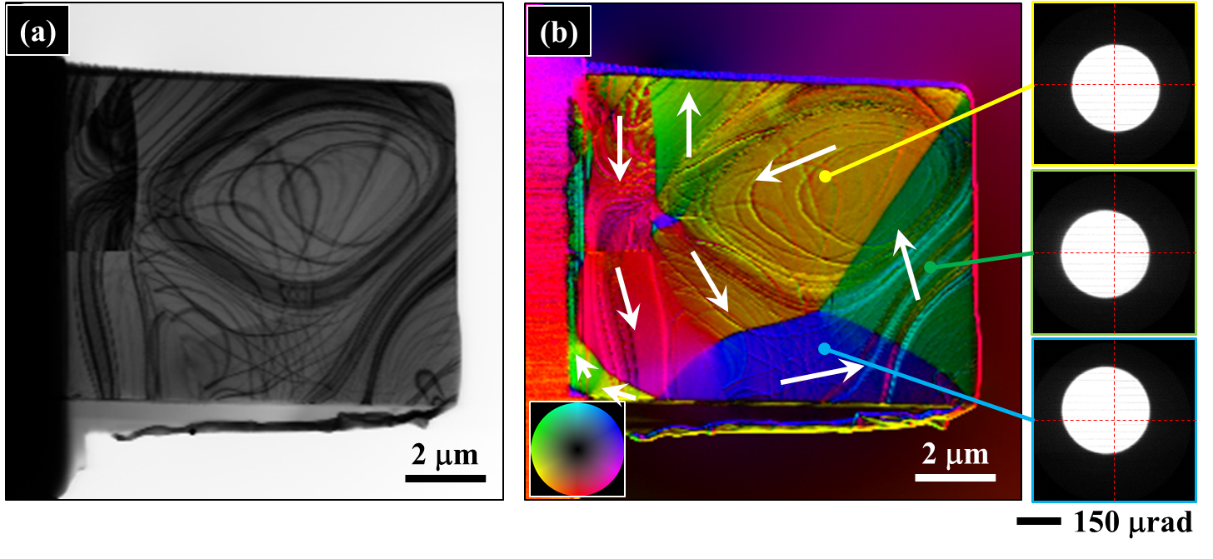
図5. 4D-STEM法で可視化したMn-Znフェライト軟磁性材料の磁区構造の例。
(a)4次元データを用いて再生したSTEM明視野像 (b) 可視化した試料の磁区構造(中央)と4次元データから抽出した試料上の3点での透過ディスク(右)。各点での磁化の方向の違いによって、電子線が異なる方向に偏向されていることが分かる。
Four dimensional-scanning transmission electron microscopy (4D-STEM) is a method in scanning transmission electron microscopy (STEM) that acquires the diffraction patterns for many probe points using a two-dimensional (2D) detector (pixel array STEM detector), creates four-dimensional (4D) data and obtains electron microscope images reflecting information from the diffraction patterns.
That is, an electron probe is scanned two-dimensionally on a specimen, and electron diffraction patterns are simultaneously recorded at each specimen position using a two-dimensional (2D) detector (Fig. 1(a)). The acquired data forms a four-dimensional (4D) data consisting of the 2D spatial position data of the specimen (x, y) and the 2D diffraction data (u, v) corresponding to each spatial position formed on the camera screen (Fig. 1(b)). From this 4D data, it is possible to visualize the distribution of crystalline phases, crystal orientations, and the directions of magnetic- and electric-fields by using the differences in the diffraction data (u, v) at specific 2D positions (x, y). It is also possible to visualize positional changes in the crystal structure by using the angle-dependent intensities of the diffraction patterns, which have not been fully used in the conventional STEM method. Fig. 2 illustrates the difference of the convergence angle of the electron probe when taking diffraction patterns. In Fig. 2(b), the adjacent diffraction disks are partially overlapped with each other. From the overlapping areas, the phase of the corresponding diffracted wave is obtained. This phase is then used to refine the structure of the specimen, which is known as ptychography. Collectively, these techniques are referred to as the 4D-STEM method.
Three analysis examples using 4D-STEM are presented below. In each case, the convergence angle of the electron beam (probe) and the magnification by the image-forming system (camera length) are different (Fig. 2). These conditions are determined according to the purpose of analysis
Example of orientation analysis of a crystalline specimen (Fig. 3).
Example of reconstruction (phase reconstruction) of a crystal structure using ptychography (Fig. 4).
Example of visualizing the magnetic field distribution in a specimen (Fig. 5).
Fig. 1. (a) 4D-STEM data acquisition method: An incident electron beam (probe) is scanned two-dimensionally on a specimen, and at each position, a two-dimensional electron diffraction pattern is recorded using a CCD or CMOS camera. (b) Schematic diagram of a four-dimensional data acquired by the 4D-STEM method.
Fig. 2. Examples of the acquisition conditions of 4D-STEM data; (a) when the convergence angle is small, (b) when the convergence angle is large, and (c) when the camera length is increased to magnify the displacements of the transmitted and diffracted wave disks.
1. Example of orientation analysis of a crystalline specimen
Fig. 3 shows an orientation analysis example of the crystal grains in the vicinity of the grain boundary triple junction of a Mn-Zn ferrite soft magnetic material using 4D-STEM data. The 4D-STEM data was acquired with a small convergence angle to separate the transmitted wave disk and diffracted wave disk as is shown in Fig. 2(a) (For details, see the term “nano-beam diffraction” in Glossary of TEM Terms.).
From the acquired 4D data, four diffraction patterns (Fig. 3(a) right) were extracted from regions A, B, C and D in the annular dark-field STEM (ADF-STEM) image (Fig. 3(a) left). It was found that the crystal orientations at regions A, B and D are different to each other, and that region C is amorphous (halo diffraction pattern of Fig. 3(a) below the middle). This indicates that an amorphous phase is formed near the intersection of the three grains (called “triple junction”).
Furthermore, as is shown in Fig. 3(b), when a specific diffraction spot is selected in the diffraction pattern and the microscope mode is switched to the image mode, the image of the grain with a specific orientation can be displayed. That is, when diffraction spots originating from the crystalline phase (B, D) are selected, the crystal grains B and D orientations are visualized. On the other hand, when the diffuse scattering region C (no diffraction spot) is selected, the amorphous phase is visualized.
Unlike conventional methods, 4D-STEM can reveal the crystal orientation at any position from the acquired 4D data.
2. Example of reconstruction (phase reconstruction) of a crystal structure image using ptychography
Fig. 4 shows an example of reconstructing a crystal structure image (phase image) of a specimen from the acquired 4D-STEM data by ptychography using a high-speed, high-sensitivity camera. The 4D-STEM data was acquired with a large convergence angle to overlap the transmitted wave disk with the diffracted wave disks, as is shown in Fig. 2(b). Fig. 4(a) shows the 3030 and 3030 diffracted wave disks, the reflections being selected from the Fourier-transform of the scanned 2D image or the real space part of the 4D data. The two diffracted wave disks overlap with the 0000 transmitted wave disk. From the overlapping areas, the amplitude and phase of the relevant diffracted wave can be obtained. The phase of the diffracted wave is shown in color and the amplitude in color intensity in Fig. 4(b). The overlapping area between the 3030 diffracted wave disk and the 0000 transmitted wave disk is shown in blue. The overlapping area between the 3030 diffracted wave disk and the 0000 transmitted wave disk is shown in red. The difference of the two colors shows that the phase is shifted byπbetween the two overlapping areas. Note that the intensity in the yellow-green area or outside the black dashed areas A and B is a noise component, so the amplitude is set to zero. Fig. 4(c) shows a crystal structure image (phase image) of the specimen which was reconstructed (inverse Fourier-transformed) using the amplitudes and phases of many reflections obtained from the overlapping areas. This method is called “ptychography”. (See the term “Ptychography” in Glossary of TEM Terms.) In the reconstructed structure image (phase image), not only the Si atoms but also the N atoms are visualized with high contrast.
3. Example of visualizing magnetic domains in a magnetic material
Fig. 5 shows an example of visualizing the magnetic domains in a Mn-Zn ferrite soft magnetic material using 4D-STEM data. The deflection of the transmitted wave disk due to the magnetic moment is used as diffraction data. To observe clearly the deflection (its magnitude and direction) of the electron beam, the diffraction pattern is magnified under a large camera length using the image-forming lens system (Fig, 2(c)).
Fig. 5(a) shows the bright-field STEM (BF-STEM) image of the specimen, which is reproduced from the transmitted wave intensity at each specimen position of the 4D data. By extracting the deflection data of the electron beam (the directions of displacement of the transmitted wave disk) for all pixels of the specimen positions from the 4D data, the magnetic domain structure (Fig. (5b)) was revealed. The arrows shown in Fig. 5(b) indicate the directions of the magnetic moments determined from the directions of the displacements of the transmitted wave disks. In this figure, the directions and the effective magnitudes of the magnetic moments, which were obtained by differential phase contrast imaging*, are additionally shown with different colors and different color intensities, respectively (see color wheel at bottom left). On the right of Fig. 5(b), the transmitted wave disks from three points on the specimen are shown, which were arbitrarily extracted from the 4D data. It is seen that the disks from these points are deflected in different directions due to the differences in the orientations of the magnetic moments (orange cross lines are drawn in the disks to make the deflection easier to see).
It is noted that since the specimen is a soft magnetic material, a closure domain structure (magnetization is closed as a whole) is seen to stabilize the magnetic domains.
*See also the term “differential phase contrast imaging” in Glossary of TEM Terms for reference.
Fig. 3. Example of an orientation analysis of the crystal grains near the grain boundary triple junction of a Mn-Zn ferrite soft magnetic material using 4D-STEM data.
Top (a): The left figure shows an ADF-STEM image. The four figures on the right show the diffraction patterns extracted at specimen points A to D from the 4D data.
Bottom (b): The left figure shows a diffraction pattern, of which intensities were obtained by integrating over the entire specimen. The four figures on the right show STEM images obtained from the diffraction spots A to D:(A) BF-STEM image and (B, C, D) DF-STEM images.
(The result was obtained by the joint research with Zentaro Akase, Associate Professor, Nara Institute of Science and Technology)
Fig. 4. Example of reconstructing the crystal structure image (phase image) of β-Si3N4 by ptychography using the 4D data. The row data was taken at the [0001] incidence using a Cs-corrected transmission electron microscope at an accelerating voltage of 200 kV. (a) The convergent-beam diffraction patterns of the 3030 and 3030 reflections, the reflections being selected from the Fourier-transform of the scanned 2D image in the 4D data. (b) Blue and red colors indicate that the phase inversion between the two diffracted waves, the phases being opposite between the two disks. (c) Crystal structure image (phase image) reconstructed by ptychography processing.
Fig. 5. Example of visualizing the magnetic domains in a Mn-Zn ferrite soft magnetic material by 4D-STEM. (a) BF-STEM image reproduced using the 4D-STEM data. (b) Visualized magnetic domain structure of the specimen (center). Three transmitted wave disks for three points on the specimen extracted from the 4D-data (right), where the electron beam for each point is deflected in a different direction due to the different orientation of the magnetic domain.
関連用語から探す
説明に「4D-STEM」が含まれている用語


