SE1
SE1
SE1
[目次:理論]
入射電子 (一次電子) によって、入射点近く、すなわち、電子プローブ径とほぼ同じ領域で、直接励起された二次電子。この二次電子は入射点付近の試料の形状や物質の違いの情報を持っており、二次電子像の形成に用いられる。二次電子のエネルギーは最大で数10 eVである。
一次電子は非弾性散乱を繰り返して試料の深部へ拡散する。試料の深部で励起された二次電子は、エネルギーが小さいので、試料内で散乱され試料表面に到達できない。二次電子が試料表面から脱出できる深さ (脱出深さ) は金属で5~10 nmであり、この深さの範囲で生成された二次電子のみが二次電子像の形成に寄与する。
下図にSE1の発生を模式的に示す。
Secondary electron(s) which are excited directly by the incident electrons (primary electrons along the incident electron path. SE1 possesses the information on the shape and constituent materials of a specimen near the incident electrons. SE1 is used to form a secondary electron image. The energy of a secondary electron is a few 10 eV at maximum.
The primary electrons repeat inelastic scattering and diffuse into the deep region of the specimen. The secondary electrons excited in the deep region do not reach the specimen surface because they have small energies and are scattered in the specimen. The escape depth, the maximum depth, from which a secondary electron can escape beyond the specimen surface, is 5 to 10 nm for most metals. Only the secondary electrons (SE1s) generated within this depth contribute to form the secondary electron image.
The schematic of the S1 generation process is illustrated below.
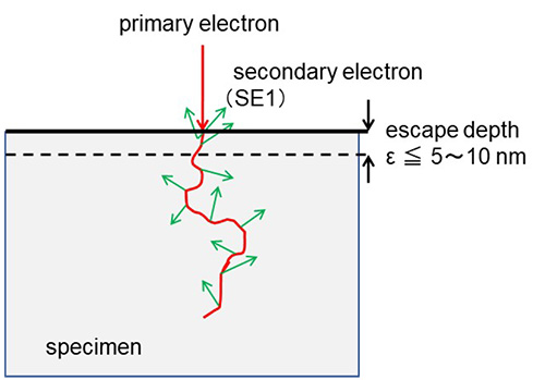
Fig. Generation process of SE1
関連用語から探す
説明に「SE1」が含まれている用語


