α フリンジ
α フリンジ
α fringe
[目次:理論(電子の散乱/回折/結像)]
結晶性薄膜試料の表面に対して斜めに入る積層欠陥面(積層欠陥を挟む二つの結晶領域に変位がある)を二波近似回折条件で撮影するとき、明視野像および暗視野像に現れる特定のコントラストを持つ縞のこと。
図1に、試料の表面に対して斜めに入る積層欠陥からの縞状のコントラストとその模式図を示す。図1(a)はチタン酸鉛(PbTiO3)の試料の表面に対して斜めに入った積層欠陥からの暗視野像である。図1(b)は図1(a)の一部分の拡大図である。図1(c)に積層欠陥とそれによって作られる縞状のコントラストを模式的に示す。格子面は積層欠陥の両側でずれている(変位している)。この変位をRとすると、回折波gに及ぼす位相角αは α=2πg・R となる。積層欠陥が試料の上下の表面と交わるところに現れる縞のコントラストが、縞の中央(試料の厚さの半分の位置)に関して、明視野では対称になるが暗視野では反対称になる。図1(b)で、両端の縞が中央に対して反対称、すなわち黒(D)と白(B)のペアになっているのが分かる。
この対称性から、2つの結晶領域間の位相角αの正負(変位の正負)、試料に対する界面の傾きの向き(右肩上がりか、左肩上がりか)が分かる(図1(c)では右肩上がり)。特に、Siなどの積層欠陥が、挿入型(extrinsic)か欠損型(intrinsic)を決めるために使われてきた。
位相角αに依存する縞のコントラストは、吸収効果を取り入れた動力学理論によって説明される。詳細は文献 Marc De Graef: Introduction to Conventional Transmission Electron Microscopy, pp499~ を参照のこと。αフリンジの名称は位相角αに由来する。
なお、像の縞の強度プロファイルの解析から、結晶領域間のずれのベクトルを定量的に測定するのは難しく、定量的な測定には、大角度収束電子回折法が用いられる。実例としては、以下の文献を参照すると良い。
- S. Yamada and M. Tanaka: J. Electron Microscopy 46 (1997) 67-74
- M. Tanaka, M. Terauchi and K. Tsuda: Convergent Beam Electron Diffraction III (1994) pp156-177, JEOL Tokyo
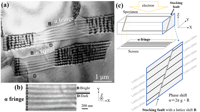
図1(a): 試料の表面に対して斜めに入った2つの積層欠陥の暗視野像。試料はチタン酸鉛(PbTiO3)。加速電圧200kV。縞の上側のフリンジは明るく (B)、下側のフリンジは暗く (D)、特徴的な非対称なコントラストを示している。なお、中央以外の部分のギザギザの縞は、積層欠陥が2枚ジグザグに重なっているために現れたものである。
図1(b): 図1(a)中の縞の一部分を拡大した図。黒(D)と白(B)のフリンジのペアがみられ, 両端(上下)が中央に対して反対称のコントラストになっているのが分かる。
図1(c): 積層欠陥を含む試料と得られる縞模様の模式図。
"α fringe" means the edge fringes showing a specific contrast of the striped interference image obtained from a stacking fault oblique to a crystalline specimen surface, which appears in the bright- and dark-field images taken at a two-wave approximation condition. (The stacking fault is a planer defect at which an atomic displacement takes place between the two crystalline regions sandwiching the fault plane.)
Figure 1 shows the striped interference image of stacking faults intersecting oblique to the specimen surface and the illustration of the α fringe. Fig.1(a) shows a dark-field image of such two stacking faults of PbTiO3. Fig.1(b) shows an enlarged image of a part of Fig.1(a). Fig.1(c) shows a schematic of the oblique stacking fault and expected striped image, the lattice planes being displaced at the staking fault.
The atomic displacement R between the lattice planes produces the phase angle α for a diffracted wave g expressed as α=2πg・R. The end stripes or fringes, which appear at the intersection between the stacking fault and the upper and lower surfaces of the specimen, exhibit symmetric contrast in the bright-field image and anti-symmetric contrast in the dark-field image with respect to the center of the striped image (to the half depth position of the specimen). The anti-symmetric contrast (nature) in the dark field image or a dark (D)- and bright (B)-fringe pair is clearly seen in Fig.1(b).
This symmetry nature reveals the sign of the phase angle α or the sign of the displacement between the two crystalline regions, and the orientation of the fault against the specimen, that is, upward to the right (as in Fig.(c)) or upward to the left. In particular, the nature of α fringe has been used to determine whether the stacking fault of Si is the extrinsic type or the intrinsic type.
The nature and formation of the striped image depending on the phase angle α is explained by the dynamical diffraction theory taking account of the absorption effect (see Reference: Marc De Graef: Introduction to Conventional Transmission Electron Microscopy, pp499~). The term "α" fringe is originated from the phase angle α.
It should be noted that it is difficult to determine quantitatively the displacement vector between the two crystalline regions from analysis of the fringe intensity profile. For quantitative analysis, it is essential to use large-angle convergent-beam electron diffraction (LACBED). The following references are referred to detailed LACBED analysis.
- S. Yamada and M. Tanaka: J. Electron Microscopy 46 (1997) 67-74
- M. Tanaka, M. Terauchi and K. Tsuda: Convergent Beam Electron Diffraction III (1994) pp156-177, JEOL Tokyo
Fig.1(a) Two striped images or α fringes oblique to the specimen surface (dark-field image of stacking faults). Specimen: PbTiO3. Accelerating voltage: 200 kV. The upper fringe of the stripe is bright (B) and the lower fringe is dark (D), showing a characteristic asymmetrical contrast. It is noted that the zigzag images appearing left and right is due to zigzag overlap of two stacking faults.
Fig.1(b) Enlarged image of a part of the stripe in Fig.1(a). A pair of dark (D) and bright (B) fringes is seen. The (top and bottom) fringes show anti-symmetric contrast nature with respect to the center of the stripes.
Fig.1(c) Schematic of a stacking fault oblique to the specimen and the striped image obtained from the fault.
関連用語から探す
説明に「α フリンジ」が含まれている用語


