オメガフィルタ
オメガフィルタ
omega filter
[目次:分光分析(EELS/EDS/電子構造)]
インコラム型のエネルギーフィルタで透過電子顕微鏡の中間レンズと投影レンズの間に組み込まれる。4個の電磁石からなる分光器は、Ω(オメガ)という文字の形に似ていることから、オメガフィルタと呼ばれる。エネルギー分散能は200keVの電子線に対して、およそ1μm/eVである。おもにフィルタ像(ゼロロス)像、ゼロロスCBED図形、エネルギーロス像を得るために使われる。
omega filter ⇒図
Ωフィルタの働きと得られるスペクトルの概念図。
エネルギーEの電子の軌道(光軸を通る軌道)を青で示し、⊿Eだけエネルギーを失った電子の軌道(エネルギー分散を起こした軌道)を赤線で示す。エネルギー分散が起きている面 (S) をスクリーンに投影すると、ロス(損失)エネルギーに対する強度分布(エネルギースペクトル)が観察される。面S上にはエネルギースリットが置かれている。
また、エネルギー分散が消滅する面、すなわちアクロマティック面 (A) をスクリーンに投影すると、エネルギー分散の無い像が観察される。その際、エネルギースリットを用いて、ゼロロスエネルギーを選択するとゼロロス像(フィルタ像とも言う)が得られ、ロスエネルギーを選択するとロス像が得られる。
(a) Siのエネルギースペクトル(加速電圧:200kV)、(b)エネルギースペクトルのラインプロファイル ⇒図
ZLPはゼロロスピーク。P1 はプラズモンロス (Ep = 16.7eV) によるピーク。P2, P3… はプラズモンの多重散乱によるピーク。L2,3 は内殻電子励起によるなだらかなピーク。
cubic-BN [110]のCBED図形(加速電圧100kV) ⇒図
アクロマティック面にできているCBED図形をそのままスクリーンに投影した図形(a)と面S上にあるエネルギースリット用いてゼロロスエネルギーを選択した図形(b)との比較。下のグラフは写真の線A-B上のラインプロファイル。
エネルギースリット無し (Unfiltered)の左図では、縞模様がぼやけて不明瞭であるが、エネルギースリットでロスエネルギー (約10eV以上) をカットした右図 (Filtered) では、縞模様が明瞭に観察されている。回折図形の定量解析を行う場合、エネルギーフィルタは必要不可欠である。
氷包埋したリポソームの像(加速電圧200kV) ⇒図
アクロマティック面にできている像をそのままスクリーンに投影した像(a)と、面S上にあるエネルギースリットを用いてゼロロスエネルギーを選択したフィルタ像(b)との比較。フィルタ像(b)では、リポソームのコントラストが増加している。
One of the in-column type energy filters, which is installed between the intermediate and projector lenses in a TEM. The filter (spectrometer) is composed of four electromagnets and has a shape of the letter “omega.” Thus, this is called “omega filter.” Its energy dispersion is approximately 1 μm/eV for a 200 kV electron beam. The omega filter is used to date to acquire filtered (zero-loss) images, energy-loss images and zero-loss CBED patterns.
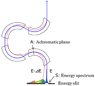
Schematic of the action of the omega filter and an acquired spectrum.
A blue curve shows the trajectory of electrons passing through the optical axis with an energy E. A red curve shows the trajectory of electrons suffered by energy dispersion with an energy loss of ⊿E. When the optical plane at which energy dispersion (S) is created is projected onto the screen, the intensity distribution against energy losses, or an energy spectrum is observed.
When the achromatic plane (A), at which energy dispersion disappears, is projected onto the screen, an image without energy dispersion is observed. In this case, if the energy slit placed on plane S is inserted to pass no energy-loss electrons, a zero-loss image (so called “filtered image”) is acquired. If the energy slit selects energy-loss electrons, an energy-loss image is obtained.
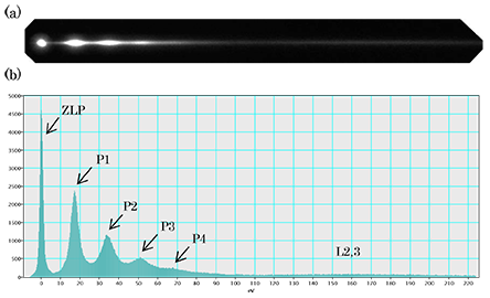
(a) Energy spectrum of Si acquired at an accelerating voltage of 200 kV. (b) Line profile of the energy spectrum. ZLP is the zero-loss peak. P1 is a peak of a plasmon loss electrons (Ep = 16.7 eV). P2, P3… are peaks produced by multiple scattering of the plasmon. Weak and broad peaks L2,3 are the spectra due to excitation of inner-shell electrons.
![cubic-BN [110]のCBED図形(加速電圧100kV)](./glossary_file/file/omega_filter_cbed.png)
CBED patterns of cubic-BN [110] acquired at an accelerating voltage of 100 kV. The two patterns were taken by projecting the CBED patterns formed at the achromatic plane onto the screen. (a) CBED pattern without using the energy slit (unfiltered pattern). (b) Filtered CBED pattern by selecting zero-loss energy with the energy slit. The graphs below the patterns are line profiles of each line A-B.
In the unfiltered pattern at the left, the patterns inside the CBED disks are unclear. To the contrary in the filtered pattern at the right, where the lost energies approximately more than 10 eV are cut, the patterns in the disks are clearly seen. The energy filter is indispensable for quantitative analysis of CBED patterns.
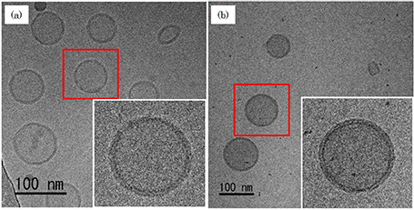
TEM images of ice-embedded liposome acquired at an accelerating voltage of 200 kV, taken by projecting the images formed at the achromatic plane onto the screen. (a) Conventional image without using the energy filter (unfiltered image). (b) Zero-loss image using the energy filter (filtered image).
It is seen that the image contrast of liposome is enhanced in the filtered image (b).
関連用語から探す
説明に「オメガフィルタ」が含まれている用語


