環状明視野法
環状明視野法
annular bright-field scanning transmission electron microscopy, ABF-STEM
[目次:理論(電子の散乱/回折/結像)]
明視野高分解能STEMの内、ダイレクトビームディスク(透過ビーム)の光軸中心部を用いずに周辺部(例12~24mrad)のみを円環状(リング状)検出器で選択的に受け、この電子の積分強度を入射電子プローブの位置に対応させて表示して高分解能原子像を得る手法。軽元素からなる原子コラムを効果的に可視化することができる。
原子番号の小さな元素からなる原子コラムでは、電子線のチャンネリング効果によって、入射光に平行な原子コラムに沿って進む電子の割合が散乱される電子に比べて大きくなる。そのため、軽元素コラムでは、円環状検出器の内側を通り抜ける電子が多くなり、結果として軽元素が効果的に黒く結像される(結像に寄与する電子の量が減少した像)。また、原子番号の大きな元素からなる原子コラムでは、電子がより高角に散乱され円環状検出器の外側を通る電子が多くなり、結果として原子位置は黒く結像される。そのため、酸素やLi原子等の軽元素の原子コラムに加えて、遷移金属等の比較的重い元素の原子コラムも同様のコントラストで観察することができる。
軽元素を可視化する方法としてHREMやBF-STEMが挙げられる。ただ、これらの手法では、原子コラムの強度が焦点はずれ量や試料の厚さに依存して大きく変化するので、正しい像解釈をするには像のシミュレーションが必要になる。一方、ABF-STEM像では(試料の厚さが非常に薄いところを除いては)試料の厚さが変化しても原子位置は常に黒く結像される。また、焦点が外れた場合でも、結像に関与する角度領域が広いため干渉効果が軽減されるので、原子位置は黒く結像され、HREMやBF-STEMに比べて解釈しやすい像になる。
SrTiO3[100]入射の高分解能STEM像 ⇒図
加速電圧: 200 kV、 入射電子線の収束角: 半角22 mrad
図(a) HAADF-STEM像。相対的に重い元素からなるSrとTi+Oコラムは輝点として明瞭に可視化されている。しかし、軽い元素であるOコラム位置では輝点を観察することはできない。検出器の取り込み角は半角90 - 170 mrad。
図(b) ABF-STEM像。HAADF像では観察することができないOコラムを暗点として明瞭に観察することができる。検出器の取り込み角は半角11 - 22 mrad。
2つの検出器の光線図の比較 ⇒図
図(a) HAADF-STEMにおける入射電子線の収束角と散乱電子線の検出器への取り込み角の関係。検出器の典型的な取り込み角はβ1 ~ 50 mrad、β2 ~ 200 mradである。高角度に散乱された非弾性散乱電子を検出する。200 kVの収差補正電子顕微鏡の場合、αは25 mrad程度である。通常、ABF検出器やLAADF検出器はHAADF検出器の下部に配置される。
図(b) ABF-STEMにおける入射電子線の収束角と散乱電子線の検出器への取り込み角の関係。入射電子線の収束半角をαとすると検出器の取り込み角は、β1はα/2、β2はαと同程度に設定する。透過波の光軸中心部を用いず周辺部のみをリング状に検出する。 200 kVの収差補正電子顕微鏡の場合、α、β1、 β2はそれぞれ25 mrad、13mrad、25 mrad程度である。
Annular bright-field scanning transmission electron microscopy (ABF-STEM) is a bright-field high-resolution STEM method which preferentially receives only the ring-shaped circumference (e.g. 12 to 24 mrad) of the direct (transmitted)-beam disk using an annular bright-field (ABF) detector, without using the central part of the bright field disk. The integrated intensities of the received electrons are displayed in synchronism with the incident probe position for acquisition of a high-resolution atomic image. The ABF method enables us to effectively visualize atomic columns composed of light atoms.
In these light-element atomic columns, the intensities of electrons which travel along the atomic columns parallel to the incident beam, become higher than the scattered electrons due to the electron channeling effect. Thus, the electrons which are incident on the light atomic columns increase to pass through the center hole of the ABF detector. As a result, light elements are effectively imaged as dark spots (image formed by smaller quantity of electrons). On the other hand, the electrons which are incident on the heavy atomic columns increase to scatter at high angles outside of the ABF detector. As a result, heavy atomic columns are also imaged as dark spots. Thus, the ABF method enables us to observe both the atomic columns of relatively heavy elements (transition metals, etc.) and light elements (O, Li, etc.) with the same contrast.
HREM and BF-STEM have long been used to visualize atomic columns. However, those two methods necessitate image simulations for correct image interpretation because the intensity of the atomic column largely depends on the defocus amount and specimen thickness. In the ABF-STEM image, (except for extremely thin specimen) the atoms are always imaged as dark spots irrespective of the variation of specimen thickness. Even in the image formed with a certain defocus, atoms are still imaged as dark spots because the incident electrons over a certain angular range reduce the interference effect of each electron. This makes an easy interpretation of the ABF image compared to the HREM and BF-STEM images.
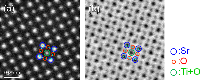
High-resolution STEM images of SrTiO3 taken at the [100] incidence. (Accelerating voltage: 200 kV, Convergence semi-angle of the incident electron beam: 22 mrad)
Fig.(a) HAADF-STEM image taken with an acceptance semi-angle of the detector 90 to 170 mrad. Sr columns and Ti + O columns, which are composed of relatively heavy atoms, are clearly visualized. However, the light-atom O columns cannot be observed as bright spots.
Fig.(b) ABF-STEM image taken with an acceptance semi-angle of the detector 11 to 22 mrad.
The light-atom O columns, which cannot be seen in the HAADF image, are clearly observed as dark spots.
Comparison of Ray diagrams of two detectors
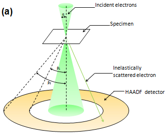 Fig.(a) Relationship between the convergence semi-angle of the incident electron beam and acceptance semi-angles of the detector for HAADF-STEM. Typical inner and outer semi-angles of the detector are respectively β1 = ~50 mrad and β2 = ~200 mrad, detecting inelastically scattered electrons at high angles. The value of the convergence semi-angle α is approximately 25 mrad for a 200 kV Cs-corrected TEM. Usually, an ABF detector and a LAADF detector are placed below a HAADF detector. |
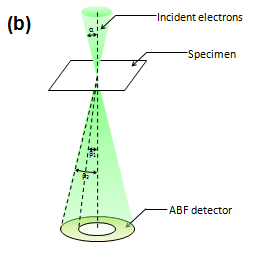 Fig.(b) Relationship between the convergence semi-angle of the incident electron beam and acceptance semi-angles of the detector for ABF-STEM. The inner and outer acceptance semi-angles of the detector are respectively taken as β1 ≒ α/2 and β2 ≒ α, where a is the convergence semi-angle. It should be noted that the only peripheral part of the bright field disk (without the central part) is used for ABF-STEM. In the case of a 200 kV Cs-corrected TEM, α, β1 and β2 are respectively ~25 mrad, ~13 mrad and ~25 mrad. |
関連用語から探す
説明に「環状明視野法」が含まれている用語


