菊池図形
菊池図形
Kikuchi pattern
[目次:理論(電子の散乱/回折/結像)]
入射電子が、結晶性試料内で原子の熱振動による非弾性散乱(熱散漫散乱)を受けた後にブラッグ反射(弾性散乱)を起こすことによって生じる図形。非弾性散乱を受けた電子の進行方向は広い角度にわたって分布するので、ブラッグ反射は斑点でなく、ある結晶面の表面と裏面の反射(例えば200反射と-200反射)による明暗の一対の線(菊池ライン)になる。明暗の線は、入射線の方向に近い線は周辺に比べて強度が低く(暗く、defect)、遠い線は強度が高く(明るく、excess)なる。
低次の反射を強く励起する場合は、強い動力学効果によって表面と裏面による反射線の間に広がる強度が高いバンド(菊池バンド)が形成される。
結晶性がよく試料が厚いほど、菊池図形は明瞭に現れる。菊池ラインをブラッグ反射スポットの上に来るように結晶の傾きを調整することによって、結晶の方位を精確に合わせることができる。
Kikuchi Pattern⇒図
(a)菊池ライン:結晶内のある点Oで非弾性散乱した電子が、入射電子の方向Iに対してかなり傾いた結晶面の表の面Fと裏の面Bでブラッグ反射を起こすと、ブラッグ反射位置 (方向) 1, 2に暗線と明線のペアが生ずる。これを菊池ライン(KL)という。電子線の入射方向Iに近い方(1)の菊池ライン(KL)は、B面によって反射された波とF面を透過してきた波から作られ、その強度は、その周辺に比べて低い(暗線defect)。電子線の入射方向Iから遠い方(2)の菊池ライン(KL)は、F面によって反射された波とB面を透過してきた波から作られ、その強度は周辺に比べて高い (明線excess)。
点Oで生ずる非弾性散乱の振幅は、入射線の方向に近い低散乱角側で大きく、散乱角が大きくなるにつれて小さくなる。(入射波の方向に近い方向に非弾性散乱された電子によって)結晶の表の面Fからのブラッグ反射は、強い明線(excess KL)と強い暗線(defect KL)を形成する。(入射波の方向から遠い方向に非弾性散乱された電子によって)結晶の裏の面Bからのブラッグ反射は、表の面Fからの効果を打ち消すように働く。しかし、裏の面による強度は小さく打消しの効果は小さいので、明線の菊池線(excess KL)が入射波から遠い側(2)に、暗線の菊池線(defect KL)が入射波に近い側(1)に形成される。
(b)菊池ラインから菊池バンドへの移行:入射電子の方向Iに対して結晶面の傾きが小さくなると、反射面Fと反射面Bに入射する非弾性散乱の振幅の差が小さくなり、菊池ラインの釣鐘型の強度は低くなり、釣鐘型の左右対称性が崩れ非対称な強度(分散型の強度)が現れ始める。
(c)菊池バンド:入射電子の方向Iに対して結晶面が対称的になると、非弾性散乱の振幅はブラッグ反射1と2に対して等しくなり、釣鐘型の強度はなくなり、強い動力学効果のために分散型の強度が現れる。反射位置1と2に挟まれた帯状の領域では周りに比べて強度が高くなる。この強度の高い帯を菊池バンド(KB)という。
Kikuchi pattern obtained from a Si single crystal⇒図
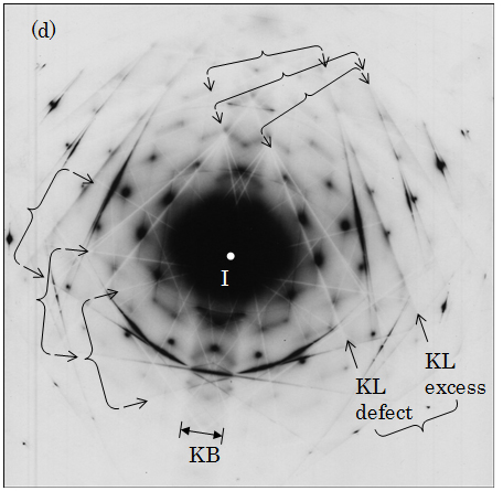
(d)Si単結晶からの菊池図形:高次反射による多くの菊池ラインのペアが見られる。対称な入射付近では、G=220反射と-G=-2-20反射の間に菊池バンドが見られる。明暗の線は、入射線の方向に近い線は周辺に比べて強度が低く(暗く、defect)、遠い線は強度が高く(明るく、excess)なる。(但し写真では明暗を反転させて表示している)
The Kikuchi pattern is a diffraction pattern produced by Bragg reflections of inelastically scattered (thermal diffuse scattering) electrons in a specimen. Since the inelastically scattered electrons distribute over large angles, the Bragg reflections by the inelastically scattered electrons do not form diffraction spots but form a pair of excess and defect lines (Kikuchi lines) respectively by hkl and -h-k-l reflections. The low-intensity (defect) Kikuchi lines appear near side of the direction of the incident beam, whereas the high-intensity (excess) Kikuchi lines appear far side of the direction.
When low-order reflections hkl and -h-k-l are strongly excited, a high-intensity (excess) band (Kikuchi band) is formed between the reflections due to a strong dynamical diffraction effect. Kikuchi lines appear sharply for a highly perfect and thick crystal. Kikuchi patterns are effectively used for precise adjustment of a crystal orientation by tilting the crystal for the Kikuchi lines to locate on the Bragg reflection spots.
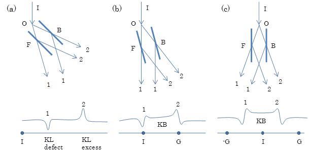
(a) Kikuch lines: When the electrons inelastically scattered at a certain point O in a crystal cause Bragg reflections from the front face (F) and the back face (B) of a crystal plane quite inclined against the direction of incident electrons I, a pair of defect intensity and excess intensity lines which are called Kikuchi lines (KL) are produced at the positions (directions) of the Bragg reflections 1 and 2. The intensity of Kikuchi line (1) near side of I is lower than that of the surrounding area (directions). To the contrary, the intensity of Kikuchi line (2) far side of I is higher than that of the surrounding area (directions).
The amplitude of the electrons inelastically scattered at the point O is large at low scattering angles and becomes small as the scattering angle increases. The Bragg reflection (2) from the front face (F) of a crystal plane due to the electrons inelastically scattered near the incident direction I forms strong excess and strong defect Kikuchi lines. The Bragg reflection (1) from the back face (B) of the crystal plane due to the inelastically scattered electrons far from the direction I compensates the contributions from the front face. However, since the compensation by the latter is small, the low intensity (defect) KL (1) is formed near side of I, and the high intensity (excess) KL (2) is formed far side of I.
(b) Transformation from Kikuch lines to Kikuchi band: When the inclined angle of the crystal plane becomes small with respect to the direction of the incident electrons I, the difference of the amplitudes of inelastically scattered electrons incident on the reflection planes F and B becomes small. As a result, the bell-shaped intensity of Kikuchi lines becomes low, the symmetrical feature is lost, but an asymmetric (dispersion type) intensity starts to appear.
(c) Kikuchi band: When the crystal plane becomes symmetric with respect to the direction of the incident electrons (I), the amplitudes of inelastically scattered electrons become equal for the Bragg reflections 1 and 2. As a result, the bell-shaped intensity vanishes and then, the dispersion type intensity is formed due to a strong dynamical diffraction effect. In the angular region between the positions (directions) 1 and 2, the intensity becomes higher than outside the region. This high intensity band is called Kikuchi band (KB).
(d) Kikuchi pattern obtained from a Si single crystal: Many pairs of Kikuchi lines due to high-order reflections are seen. In the vicinity of a symmetric incidence, a Kikuchi band is seen between “G = 220 reflection” and “G = -2-20 reflection”. The low-intensity (defect (dark)) Kikuchi lines appear near side of the incident beam direction, whereas the high-intensity (excess (bright)) Kikuchi lines appear far side of the direction. (However the Kikuchi pattern below is shown with reversal of bright and dark.)
関連用語から探す
説明に「菊池図形」が含まれている用語


