元素マッピング
元素マッピング
element (elemental) mapping
[目次:分光分析(EELS/EDS/電子構造)]
元素マッピングの主な手法には、EELSを用いるものと、EDSを用いるものの2つがある。EELSの場合、内殻電子の励起スペクトル(内殻電子励起スペクトル)中の各元素に固有の損失エネルギーをエネルギーフィルタで選択して像モードにすることにより、各元素の分布像を得る。(この説明はTEM-EELSに準拠しているが、スキャンニング法によるSTEM-EELSもある。) EDSの場合は、電子ビームを二次元走査しながら各元素に固有のX線の強度を測定し、その強度に応じた輝度変調を、走査信号と同期させてコンピュータモニタ上に表示させることにより、二次元元素分布像を得る。
(a) EDSを用いた高空間分解能元素マップ。試料:SrTiO3、加速電圧:80kV。⇒図
電子ビームを二次元走査してX線スペクトルを取得し、元素に固有の特性X線強度 O-K, Ti-Kおよび Sr-L を走査点上に分布させた像である。RGBは各元素マップを重ね合わせたものである。
(b) STEM-EELSを用いた高空間分解能元素マップ。試料:SrTiO3、加速電圧:80kV。⇒図
電子ビームを二次元走査して内殻電子励起スペクトルを取得し、元素に固有の損失エネルギー強度 O-K, Ti-Lおよび Sr-M を走査点上に分布させた像である。RGBは各元素マップを重ね合わせたものである。
(c) オメガフィルタを用いたTEM-EELSにより得られた元素マップ。試料:SiC/Si3N4、加速電圧:1250kV。⇒図
TEM-EELSで内殻電子励起スペクトル(図右下)を取得し、元素に固有の損失エネルギー強度 C-K, N-K または O-Kをスリットで選択して得た各元素のエネルギーフィルタ像である。RGBは各元素マップを重ね合わせたものである。
TEM-EELSを用いた元素マッピングは視野数μm程度の広視野低倍像で用いられることが多い。
"Element (elemental) mapping" is carried out by using EELS spectra and EDS spectra. In the case of EELS mapping, the loss energy characteristic of each element in a core-loss spectrum is selected with the energy slit at the EELS mode, and then the mapping of the element is obtained by switching to the image mode. (This explanation is based on TEM-EELS but there is STEM-EELS method which uses the scanning technique like EDS mapping.) In the case of EDS mapping, the X-ray intensities characteristic of each element are measured while the electron beam is two-dimensionally scanned on the specimen, and then brightness modulations corresponding to the X-ray intensities are displayed on a computer monitor synchronized with the scanning signals. As a result, a two-dimensional distribution image of an element is obtained.
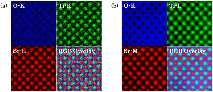
(a) High spatial resolution elemental maps acquired by EDS. Specimen: SrTiO3, Accelerating voltage: 80 kV.
X-ray spectra are acquired by two-dimensionally scanning the electron beam over the specimen, and intensities of characteristic X-rays of O-K, Ti-K and Sr-L are displayed on the corresponding scanning points. RGB map is the overlay of each elemental map.
(b) High spatial resolution elemental maps acquired by STEM-EELS. Specimen: SrTiO3, Accelerating voltage: 80 kV.
Core-loss spectra are acquired by two-dimensionally scanning the electron beam over the specimen, and intensities of energy-loss electrons of O-K, Ti-L and Sr-M are displayed on the corresponding scanning points. RGB map is the overlay of each elemental map.
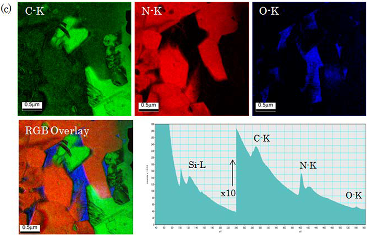
(c) Elemental maps acquired by TEM-EELS using an Omega filter. Specimen: SiC/Si3N4, Accelerating voltage: 1250 kV.
Core-loss spectra (bottom-right figure) are acquired by TEM-EELS. Energy-loss intensities of C-K, N-K or O-K which are characteristic of respective elements are chosen with the energy selection slit. Then, the energy filtered images of the elements C, N and K are displayed as elemental maps. RGB map is the overlay of each elemental map. Elemental mapping using TEM-EELS enables to acquire a wide-field low-magnification elemental map image over an area of a few μm.
関連用語から探す
説明に「元素マッピング」が含まれている用語


