収束電子回折
収束電子回折
convergent-beam electron diffraction, CBED
[目次:理論(電子の散乱/回折/結像)]
入射電子線を円錐状に絞って直径10nm以下の微小領域に照射し、ディスク状の回折図形を得て、結晶構造の定性/定量解析をする手法。ディスク内には回折条件の変化に対する強度分布(ロッキングカーブ)が得られる。試料の厚さ、格子定数、結晶の対称性(点群、空間群)、格子欠陥の同定ができるだけでなく、構造精密化(原子座標、温度因子、低次の構造因子の決定(ポテンシャル分布))ができる。大角度収束電子回折法(LACBED)を用いると、格子欠陥の同定が容易におこなえ、多層膜の界面領域での歪み(および転位)を高精度で決定できる。エネルギーフィルタを使うと、一層高精度の解析ができる。
CBED (a)(b)⇒図
(a) 通常の電子回折 (制限視野回折)
平行な電子線を試料に照射すると、対物レンズの後焦点面にスポット状の回折パターンが得られる。それを結像レンズ系で拡大してスクリーン上に映し出す。図では結像レンズ系による結像を省略している。
(b) 収束電子回折
電子線を絞って試料に照射すると、対物レンズの後焦点面にディスク状の回折パターンが得られる。それを結像レンズ系で拡大してスクリーン上に映し出す。
通常、隣接する回折波が互いに重ならないようにするために、収束半角αはブラッグ角θ以下に設定する。
CBED (c)(d)⇒図
(c) 通常の電子回折 (制限視野回折) の例。試料:Si [111]、加速電圧:200kV。
(d) 収束電子回折図形の例(ゼロロス像)。試料:Si [111]、加速電圧:200kV。
A method for qualitative and quantitative analysis of crystal structures from a disk diffraction pattern, acquired by illumination of a cone-shaped convergent electron beam on a small specimen area with a diameter of 10 nm or less. The CBED disk displays the intensity distribution corresponding to changes of diffraction conditions (rocking curve). The method enables us to determine not only specimen thickness, lattice parameter, crystal symmetry (point group and space group) and characteristics of a lattice defect, but also a crystal structure (refinement of atomic coordinates, Debye-Waller factors, low-order structure factors (potential distribution)). When the large-angle convergent-beam electron diffraction (LACBED) technique is applied, the characteristic feature of a lattice defect is easily and unambiguously identified and the strains (and a dislocation) at interfaces of a multi-layer material are determined with a high accuracy. The use of an energy filter allows us to conduct more accurate structure analysis.
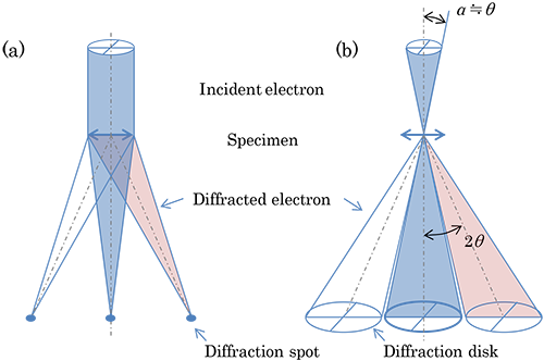
(a) Conventional electron diffraction (Selected-area diffraction)
Illuminating a parallel electron beam onto a specimen forms a spot diffraction pattern on the back focal plane of the objective lens. This diffraction pattern is magnified with the imaging lens system and then displayed on a screen. In the figure, the ray path with the imaging lens system is omitted.
(b) Convergent-beam electron diffraction
Illuminating a cone-shaped electron beam onto a specimen forms a disk diffraction pattern on the back focal plane of the objective lens. This diffraction pattern is magnified with the imaging lens system and then displayed on a screen.
In conventional CBED, the convergence semi-angle a is limited at the maximum to the Bragg angle q to avoid the overlap of adjacent diffraction disks.
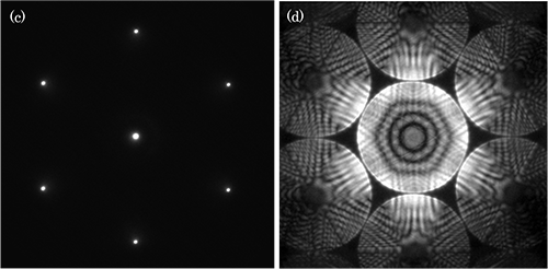
(c) Example of Conventional electron diffraction (Selected-area diffraction) pattern.
Diffraction pattern of Si [111] taken at an accelerating voltage of 200 kV.
(d) Example of Convergent-beam electron diffraction pattern.
CBED pattern of Si [111] taken at an accelerating voltage of 200 kV by eliminating energy loss electrons (Zero-loss pattern).
関連用語から探す
説明に「収束電子回折」が含まれている用語


