走査透過電子顕微鏡像
走査透過電子顕微鏡像
scanning transmission electron microscope (STEM) image
[目次:理論(電子の散乱/回折/結像)]
微小電子プローブで薄膜試料上を二段偏向系を使って走査し、試料の一点一点から出てくる透過波(または回折波)の強度を円環状の検出器で受け、その強度をプローブ走査と同期させてコンピュータモニタ上に輝点列として表示して得る像。分解能はプローブ径によって決まる。観察法には明視野法と暗視野法がある。
グラファイトの担持体上に存在するPt触媒粒子の走査透過電子顕微鏡像⇒図
明視野像(BF像)では、Pt粒子の部分は電子が高角に散乱されるために暗く見えている。環状暗視野像(ADF像)では、散乱した電子を検出しているため、Pt粒子はコントラストが逆転し明るく見えている。
"Scanning transmission electron microscope (STEM) image" is obtained as follows. A small-sized, focused electron probe is scanned over a thin specimen using the double-deflection system. The intensity of the transmitted wave (or the diffracted wave) exiting from a point on the specimen is detected with an annular detector. Then, the intensities are displayed on a computer monitor as a series of bright spots in synchronism with the scanning electron-probe. The resolution of the STEM image is determined by the probe diameter. The STEM method has two observation modes; bright-field mode and dark-field mode.
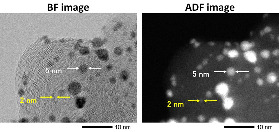
Fig. Bright-field (left) and annular dark-field (right) STEM images of Pt catalyst particles on a graphite support.
In a bright-field (BF) image, Pt particles appear dark because the incident electrons are scattered at high-angles. In an annular dark-field (AF) image, Pt particles appear bright or show reversed contrast to the BF image because the scattered electrons at high angles are received by the ADF detector.
関連用語から探す
説明に「走査透過電子顕微鏡像」が含まれている用語


