転位
転位
dislocation
[目次:結晶等(結晶構造/材料試料)]
線状の格子欠陥(線欠陥)の一種。結晶内でのある領域がすべり(ずれ)を起こしたとき、すべりを起こした領域と起こしていない領域との境界線を転位または転位線という。転位には刃状転位と螺旋転位がある。転位の周りの結晶はひどく歪んでいる。結晶の塑性は転位の運動と増殖によって説明される。
図1(a)は立方晶内に存在する刃状転位近傍の原子の並びを示す模式図である。一枚余分な格子面である余剰半面(extra half plane)が結晶に導入されており(黒線で図示)、この面の終端が刃状転位線である。転位線の周りで格子に沿って一回りする(バーガース回路:オレンジの矢印で図示)と元の格子点に戻らず、一格子分だけずれたところにくる。このずれをバーガースベクトル(赤矢印で図示)といい、転位により導入された原子位置のずれの方向と量を特徴づける量である。刃状転位におけるバーガースベクトルは転位線に垂直である。図1(b)は立方晶内に存在する螺旋転位近傍の原子の並びを示す模式図である。転位線は "ずれ" の始まる位置にあって、図の上から下に走っている。螺旋転位では、転位線の周りで格子に沿って一回りするバーガース回路は螺旋状になり、バーガースベクトル(赤矢印)と転位線は平行である。
図2は、シリコン単結晶中に存在する転位の明視野像である。転位線近傍の結晶領域が電子線を散乱しているため、明視野では黒い線状に観察されている。図3は、SrTiO3の小傾角粒界を[001]方向から観察した原子分解能暗視野STEM像である。中央部分の結晶粒界に刃状転位が並んでおり、両側の結晶はお互い対しに少し傾いている。
図1 (a)刃状転位の模式図 (b)螺旋転位の模式図 ⇒図1
図2 シリコン単結晶での転位の明視野像。加速電圧: 200 kV。 ⇒図2
(a)黒い線は、試料の表面に平行に導入された転位線。
(b)黒いギザギザの線は、試料の表面に対して斜めに導入された転位。ギザギザのコントラストは動力学的回折効果によって起こっている。
図3 (a)SrTiO3の小傾角粒界に並んだ粒界転位を[001]方向から観察した原子分解能暗視野STEM像。(試料:東京大学幾原研究室提供) ⇒図3
(b)粒界に沿った結晶面を選択的に表示し、刃状転位を明示した。
(c)刃状転位の模式図(灰色の丸は原子カラムを示す)
"Dislocation" is a linear or one dimensional defect in a crystal. When a part in a crystal is displaced against the other part, the line at which the displacement is starting is called a dislocation or a dislocation line. There are two types of dislocations, or edge dislocations and screw dislocations. The crystal around the dislocation is highly strained. Plasticity of a crystal is explained by motion and multiplication of dislocations.
Fig. 1(a) schematically shows the atomic arrangement near an edge dislocation of a cubic crystal. An extra lattice plane (called an extra half plane) is shown by a black line. The end line of the extra half plane is the edge dislocation or edge dislocation line. Suppose a circuit along the crystal lattice around the dislocation line (Burgers circuit: indicated by yellow lines with allows), the end of the circuit after one round does not come back to the original lattice point but comes to the next lattice point. This displacement is termed the Burgers vector (indicated by a red allow), which characterizes the direction and amount of the atomic displacement caused by the dislocation. The Burgers vector (shown by a red line) of the edge dislocation is perpendicular to the dislocation line.
Fig. 1(b) schematically shows the atomic arrangement near a screw dislocation. The screw dislocation (line) exists at the start (or end) line of the displacement and runs from the top to the bottom of the figure. The Burgers circuit in this case is seen to be spiral. The Burgers vector of the screw dislocation is parallel to the dislocation line (indicated by a red allow).
Fig. 2 shows a bright-field image of dislocations in a silicon crystal. The dislocations (lines) are seen to be dark (black) lines because the regions near the dislocations come into a Bragg reflection. Fig. 3 shows a [001] atomic-resolution dark-field STEM image of a small-angle grain boundary of SrTiO3. Edge dislocations are seen to be arranged along the grain boundary, creating a small orientation change between both sides of the crystal.
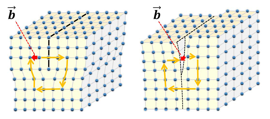
Fig. 1.(a) Schematic of edge dislocation. (b) Schematic of screw dislocation.
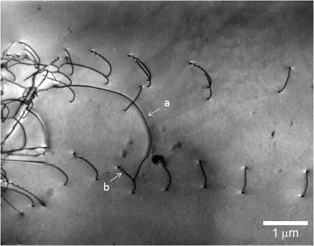
Fig. 2. Bright-field image of dislocations in a silicon crystal taken at an accelerating voltage of 200 kV.
(a) A black line (indicated by arrow "a") shows a dislocation line running parallel to the specimen surface.
(b) A black zigzag line (indicated by arrow "b") exhibits a dislocation running oblique to the specimen surface. The zigzag contrast is created by a dynamical diffraction effect.
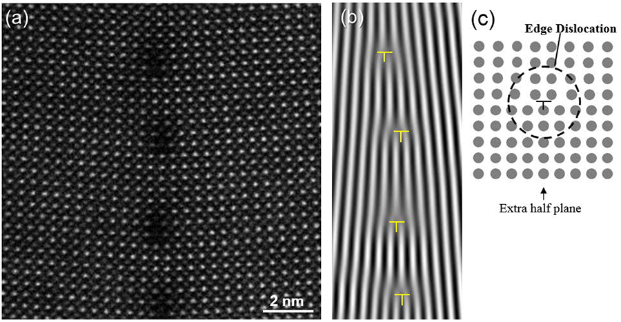
Fig. 3
(a) [001] atomic-resolution dark-field STEM image of dislocations on a small-angle grain boundary of SrTiO3 taken at an accelerating voltage of 200 kV. (Specimen courtesy: Prof. Y. Ikuhara, The University of Tokyo)
(b) Edge dislocations are clearly visualized by selectively displaying crystalline planes along the grain boundary.
(c) Schematic of the edge dislocation (gray circles indicate atomic columns).
関連用語から探す
説明に「転位」が含まれている用語


