ビームロッキング法
ビームロッキング法
beam-rocking technique
[目次:照射系(電子銃/高圧系)]
入射電子線を試料上の一点に固定し入射角をある角度範囲に亘って二次元的に振る(揺らす)方法。すなわち、二段偏向系を用いて、一段目のコイルで電子ビームを偏向し、それに連動して二段目のコイルで光軸と平行に振り戻し、対物レンズの前磁場でビームを試料上の同じ点を照射する(図1)。これを、直交する二つの偏向方向(x,y)について、ある角度範囲にわたって行う。 ALCHEMI(アルケミ)信号のx,y方向の角度変化や大角度収束電子回折図形を得るのに使われる。実際にビームロッキング法を用いて取得した像を図2に示す。
図1 ビームロッキング法の模式図
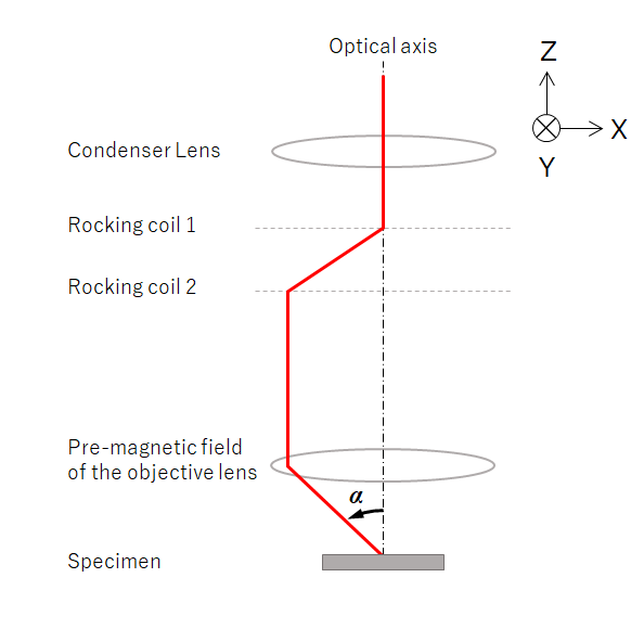
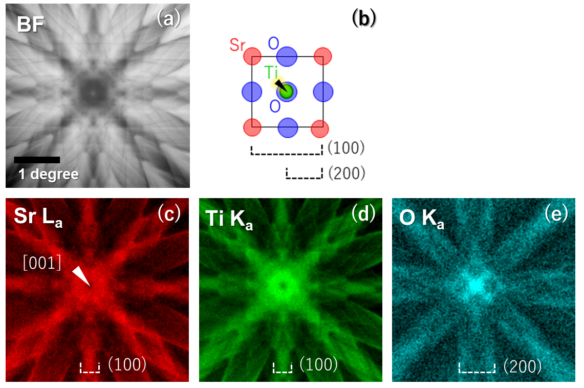
図2 試料SrTiO3でのビームロッキング図形。[001]入射、加速電圧300 kV。
結晶性試料の場合、ビームロッキング法によりビームを試料の一点に対して傾斜させると、同じ測定点でもビームの入射角度の違いによって得られる信号量が変化する。
(a) 明視野でのビームロッキング図形
(b) SrTiO3を[001]方向に投影したときの原子配置図
(c)-(e) ビームロッキング法とEDSを組み合わせて取得したビームロッキング図形。(c) はSr-Lα、(d)はTi-Kα、(e)はO-Kαの特性X線を用いたビームロッキング図形。
ビームロッキングによる特性X線強度のパターンは元素ごとに異なる。中心の[001]晶帯軸入射では軸チャンネリングと言う現象が起き、強度がSrとTiでは弱く、Oでは強い。高角度側ではアジマス方向の強度変化を見ると、SrとTi のパターンでは(100)面に対応する狭い強度の帯(バンド)が見られるのに対して、Oでは(200)面に対応した広いバンドが見られる。これは、Oの原子面の間隔が、Sr、Tiの原子面の間隔の半分になっているためである。
[付録]軸チャンネリングの強度について
パターンの中心、すなわち晶帯軸上で、Oのパターンでは明るく、Sr、Tiのパターンでは暗い。軸チャンネリングの強度は、元素種や、入射電子線の加速度に依存する。構造を仮定して結晶内を通る電子波(ブロッホ波)の位置による強弱の変化をシミュレーションすることで、試料の原子位置に関する情報が得られる。例えば添加元素の占める位置を同定できる。[1][2]
参考文献
[1] M. Ohtsuka, S. Muto, K. Tatsumi, Y. Kobayashi, and T. Kawata, Microscopy 65, 127 (2016).
[2] S. Muto and M. Ohtsuka, Progress in Crystal Growth and Characterization of Materials 63, 40 (2017).
A technique that two-dimensionally rocks the incident electron beam over a certain angular range at fixing the beam to a single point on the specimen.
Using a two-stage-deflection beam system, the electron beam is deflected by the first-stage coils and synchronously deflected back parallel to the optical axis by the second-stage coils, and is illuminated at the same specimen position by the prefield of the objective lens (Fig. 1). This is conducted over a certain angular range for two orthogonal deflection directions (x, y).
The technique is used to observe angular variations of ALCHEMI (atom-location by channeling-enhanced microanalysis) signals in the x, y directions, and to obtain LACBED (large-angle convergent-beam electron diffraction) patterns. Angular variations of ALCHEMI signals acquired by the technique are shown in Fig. 2.
Fig. 1. Schematic of the beam-rocking technique.
Fig. 2. Beam-rocking ALCHEMI patterns obtained from SrTiO3. [001] incidence at an accelerating voltage of 300 kV.
In the case of a crystalline specimen, when the beam is tilted against a single point on the specimen by the beam-rocking technique, the obtained signal changes depending on the incidence angle of the beam even from the same measurement point.
(a) Beam-rocking pattern in the bright field.
(b) Atomic arrangement of SrTiO3 projected in the [001] direction.
(c)-(e) Beam-rocking patterns of characteristic X-rays obtained by a combination of the beam-rocking technique and EDS. (c) Sr-Lα, (d) Ti-Kα and (e) O-Kα.
Beam-rocking patterns of the characteristic X-rays are different for the respective elements. At the [001] zone-axis incidence at the center of the patterns, a phenomenon called axial channeling occurs, where the intensity is weak for Sr and Ti and strong for O.
At high scattering angles in the azimuth direction, the intensity variation in the azimuth direction shows narrow intensity bands corresponding to the (100) plane in the Sr and Ti patterns, whereas a broad band corresponding to the (200) plane is seen in the O pattern. This is because the spacing of the atomic plane of O is half the spacing of the atomic planes of Sr and Ti.
Appendix: Axial channeling intensity
At the center of the pattern, i.e. on the zone axis, it is brighter for an O pattern and darker for Sr and Ti patterns. The intensity of the axial channeling depends on the element species and the acceleration of the incident electron beam. When the positional intensity changes of the electron wave (Bloch wave) running in a crystal are calculated for given crystal structures, information about the atomic positions of the specimen can be obtained. For an application example, the positions occupied by additive elements can be identified. [1] [2]
References
[1] M. Ohtsuka, S. Muto, K. Tatsumi, Y. Kobayashi, and T. Kawata, Microscopy 65, 127 (2016).
[2] S. Muto and M. Ohtsuka, Progress in Crystal Growth and Characterization of Materials 63, 40 (2017).
関連用語から探す
説明に「ビームロッキング法」が含まれている用語


