表面プラズモン
表面プラズモン
surface plasmon
[目次:分光分析(EELS/EDS/電子構造)]
金属の表面や金属と誘電体(真空も含む)の界面に荷電粒子線や光を照射すると、表面や界面に電荷が誘起される。この電荷が作る電場を駆動力として、表面あるいは界面の電荷は縦波振動を起こす。これを表面プラズモンという。
【表面プラズモンの生成】
表面電荷によって生じた電場は、表面に平行な成分と垂直な成分を持つ(図1(a))。表面に平行な電場成分(Ex)は電荷の縦波振動の駆動力となる。一方、表面に垂直な電場(Ez)の時間変化は、表面に沿った電磁波を誘起する。この電磁波の周期と一致する縦波が促進され伝播する。このようにして表面プラズモンが生成される。表面プラズモンは、金属表面からの深さとともに急激に減衰する。表面プラズモンは体積プラズモンとは異なり、電子線だけではなく、光でも観測できる。その理由は、表面に垂直な電場が表面プラズモンに対して横波成分であり、外からの電磁波はこの横波成分と相互作用を起こすからである。
【表面プラズモンの式】
金属—誘電体界面で、金属側と誘電体側の界面に垂直な電場成分をそれぞれ Ez=0- 、Ez=0+ と表す。金属側と誘電体側での電束密度が等しいことから εMEz=0- = εd Ez=0+ となる。ここで、εMとεdはそれぞれ金属と誘電体の誘電率である。図1(b)から -Ez=0- =Ez=0+ であるから、
・・・(1)
が得られる。金属の誘電率 εM を自由電子モデルによる誘電関数 εM (ω)=1-(ωP ⁄ ω)2 に置き換える。
ここで、 は体積プラズモンの角振動数である。(1)式をωについて解くと、表面プラズモンエネルギーESは
・・・(2)
となる。ここで EP=ћωP は体積プラズモンエネルギーである。金属と真空との界面での表面プラズモンエネルギーは、真空の誘電率が εd=1 であることから、 となる。
⇒図1
(a) 金属の表面プラズモンの模式図。外からの荷電粒子や光によって金属表面に正 (+) と負 (−) の電荷が誘起される。この電荷による電場 (図中 Ex (z=0±)) を駆動力として、表面の自由電子は縦波振動する。
(b) 金属—誘電体 (真空を含む) の界面に垂直な電場成分 Ez=0± と平行な成分 Ex (z=±0)。電束密度の縦成分の連続 εMEz=0- = εdEz=0+ と、電場の横成分の連続が満たされている。
【実験で得られた表面プラズモン】
図2は、電子エネルギー損失分光(EELS)によって得られたアルミニウムのスペクトルである。通常アルミニウムの表面は酸化膜で覆われている。15eVのピークは体積プラズモンによるものである。7eVに表面プラズモンのピークがみられる。アルミニウム酸化膜(Al2O3)の誘電率は εd=3.7なので、表面プラズモンエネルギーは ES=6.9 eVと計算され、実験値と良く一致する。
⇒図2
AlのEELSスペクトル。15eVのピークは体積プラズモン。7eVのピークが、AlとAlの表面酸化物との界面での表面プラズモン。
d電子を含む金属(Ag, Auなど)では、予想される表面プラズモンエネルギーとほぼ同じエネルギー位置でd電子のバンド間遷移が起き、表面プラズモンはバンド間遷移と強く相互作用する。そのため簡単な(2)式は適用できず、表面プラズモンは(2)式で計算される値よりも低エネルギー側に現れる。シリコンやGaAsなどの半導体では、(2)式で計算されるエネルギー値に表面プラズモンピークが観測される。しかし、表面プラズモンはバンド間遷移によってエネルギーを失い、振動は減衰しピークはブロードになる。ダイヤモンドやイオン結晶など、価電子が強く束縛されている絶縁体では、バンド間遷移によるスペクトルが優勢になり、表面プラズモンは弱いバックグラウンドとなって観測は困難になる。
なお、ナノメートルオーダーの微小な金属粒子や金属ワイヤーの表面においても、表面プラズモンが誘起される。この場合は、微小粒子やワイヤーの形状に依存する固有振動モード(定在波)として、表面電荷の疎密波が誘起される。波が微小粒子に閉じ込められていることから、局在プラズモンとも呼ばれる。
(東北大学多元物質科学研究所 佐藤庸平准教授による)
When a metal surface or an interface between a metal and a dielectric material (with vacuum) is irradiated by a charged-particle or a light wave, electric charges are induced at the surface or the interface for generating an electric field. With this electric field as a driving force, the charges on the surface or the interface induce longitudinal oscillations. This phenomenon is called "surface plasmon".
[Creation of surface plasmon]
The electric field generated by the surface charges possesses the components parallel and vertical to the surface (Fig. 1(a)). The electric-field component parallel to the surface (Ex) acts as a driving force to induce longitudinal oscillations. On the other hand, the change in time of the electric-field component vertical to the surface (Ez) induces electromagnetic waves along the surface. The longitudinal wave that matches the periodicity of these electromagnetic waves is enhanced and propagates. As a result, a surface plasmon is created. The surface plasmon is abruptly attenuated as the depth from the surface is large. Unlike the volume plasmon, the surface plasmon is observed with not only an electron wave but also a light wave. This is due to the fact that, the electric field vertical to the surface corresponds to the transverse wave component against the surface plasmon, and the external electromagnetic waves interact with the transverse wave component.
[Equations of surface plasmon]
For the interface between a metal and a dielectric material, the electric-field components vertical to the metal side and the dielectric material side are expressed as Ez=0- 、Ez=0+, respectively. Since the electric flux densities of the metal side and the dielectric material side are equal, εMEz=0-=εdEz=0+ is given. Here, εM and εd are the dielectric constant for metal and that for dielectric material, respectively. As shown in Fig, 1(b), -Ez=0-=Ez=0+, and thus
・・・(1)
is obtained. Then, the dielectric constant for metal εM is replaced by the dielectric function εM (ω)=1-(ω_P/ω)2 based on the free electron model. Here, is the angular frequency of the surface plasmon. When the equation (1) is solved for ω, the surface plasmon energy ES is given by the following equation.
・・・(2)
Here, EP=ћωP corresponds to the volume plasmon energy. The surface plasmon energy of the interface between a metal and a vacuum is because the dielectric constant of the vacuum is εd=1.
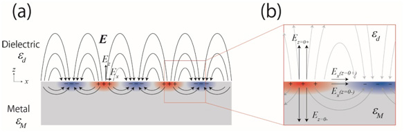
Fig. 1 (a) Schematic of surface plasmon for metal. Due to an external charged-particle or a light wave, the positive (+) and the negative (–) charges are induced. With an electric field generated by these charges (Ex (z=0±) in Fig. 1) as a driving force, a longitudinal oscillation wave of free electrons is created. (b) Illustration of the electric-field component vertical to the interface between a metal and a dielectric material (with vacuum) Ez=0± and the electric-field component parallel to this interface Ex (z=±0). Both of the continuity for the vertical component of the electric flux density εMEz=0-= εdEz=0+ and the continuity of the parallel component of the electric field are satisfied.
[Experimentally-obtained surface plasmon]
Fig. 2 shows a spectrum of aluminum (Al) acquired by electron-energy loss spectroscopy (EELS). In general, the surface of Al is coated by an oxide film. A spectral peak at 15 eV is due to the volume plasmon. A peak at 7 eV created by the surface plasmon is also seen. Since the dielectric constant of an Al oxide film (Al2O3) is εd=3.7, the surface plasmon energy is calculated to be ES=6.9 eV, which shows a good agreement with an experimental value.
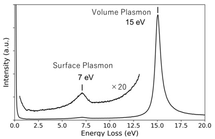
Fig. 2 EELS spectrum of Al. A peak at 15 eV is due to the volume plasmon. A peak at 7 eV is created by the surface plasmon which originates from the interface between Al and an Al oxide.
In metals containing d electrons (Ag, Au, etc.), the interband transitions of d electrons takes place at an energy position which is very close to that of the expected surface plasmon energy, and the surface plasmon strongly interacts with the interband transition. Thus, the aforementioned equation (2) is not applicable and the surface plasmon is seen at a lower energy side compared to the value calculated in the equation (2). In semiconductors like silicon (Si) and GaAs, the surface plasmon is observed at the energy position that is the same as the energy calculated in the equation (2). However, the surface plasmon loses its energy due to the interband transition, leading to the oscillation attenuation and a resultant broad spectral peak. In insulators (diamond, ion crystal, etc.) where valence electrons are strongly bounded, the spectral peak due to the interband transition dominates strongly in an EELS spectrum and thus, the surface plamson appears as a weak background for making its observation difficult.
It should be noted that, a surface plasmon is excited at the surface of a very small metallic particle or a metallic wire with its size being the nanometer-order. In this case, a compressional wave of the surface charge is induced as a characteristic oscillation mode (standing wave) which depends on the shape of the very small particle or the wire. Since this wave is confined in the very small particle, this phenomenon is called "localized plasmon".
(By Associate Professor Yohei Sato, Tohoku University)
関連用語から探す
説明に「表面プラズモン」が含まれている用語


