軸上幾何収差
軸上幾何収差
axial geometrical aberration
[目次:レンズ系]
幾何収差(像面における理想結像からのずれ)は、光軸からの距離rと光軸となす角度(開き角)αの関数として表される。その中で開き角αのみに依存する収差を軸上幾何収差(以下、軸上収差)と呼ぶ。なお、光軸からの距離rに、またはrとαの両方に、依存する収差を軸外幾何収差(以下、軸外収差という)という。
軸上収差の一覧を表1に示す。軸上収差は、開き角αの次数nと方位角方向の対称性で分類できる。たとえば、1次の軸対称収差はデフォーカス、1次で2回対称の収差は2回非点収差、と呼ばれる。3次の軸対称収差は球面収差と呼ばれており、ザイデルの5収差の1つとして知られている。表において空欄になっている収差、例えば、2次で2回対称の収差など、は原理的に現れない。
軸上収差があると、像面で一点に集まるはずの電子線が広がり、像の分解能が低下する(図1)。透過型電子顕微鏡(TEM)は多くのレンズで構成されているが、試料に最も近い対物レンズ(の後方磁場)を通るときのαが最も大きいため、対物レンズの軸上収差が分解能に最も影響する(図2)。高い倍率で試料の像を観察する場合(高分解能電子顕微鏡法)、観察する領域が狭くrが小さい範囲に限られるため、軸外収差を無視することができ、対物レンズの軸上収差のみを考慮すれば良い。
他方、走査透過型電子顕微鏡法(STEM法)で高い分解能の像を得るには、入射電子線を試料上にできるだけ小さく集光する必要がある。そのため、試料の直前のコンデンサーレンズ(実際には対物レンズの前方磁場)の軸上収差を小さくすることが重要になる(図1)。
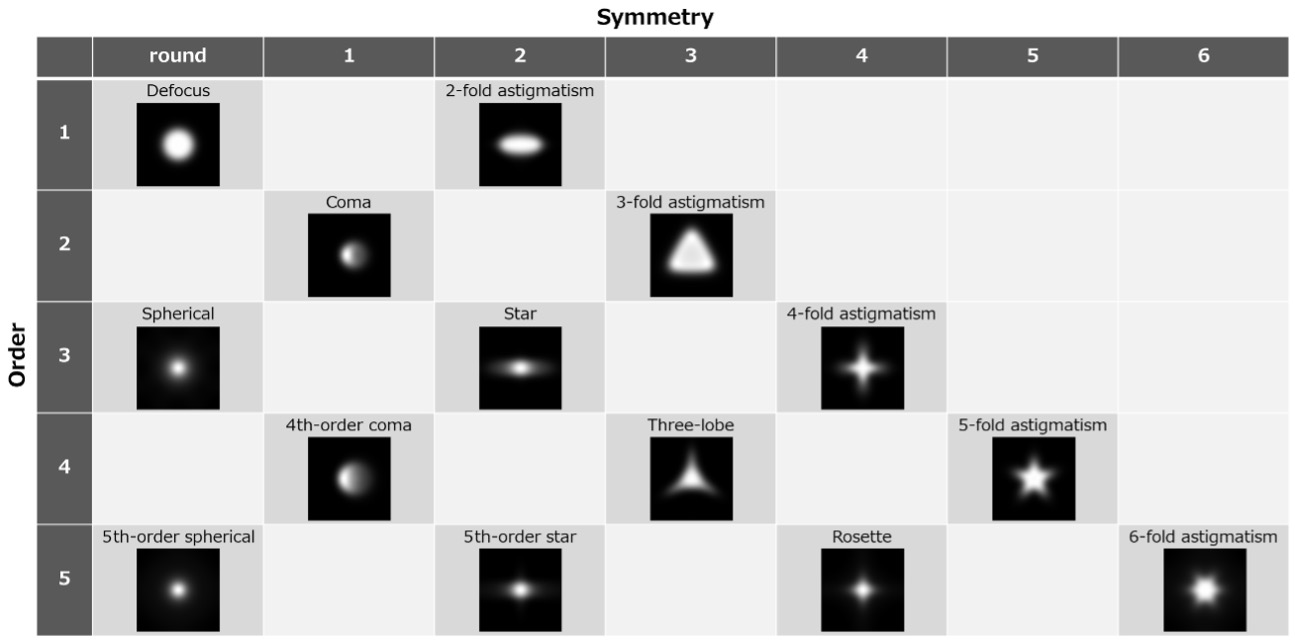
表1. 軸上幾何収差の一覧。縦方向に開き角αの次数nを、横方向に方位角方向の対称性を与えて収差を分類した。各収差によるSTEMにおける電子線プローブのぼけ方を示した。
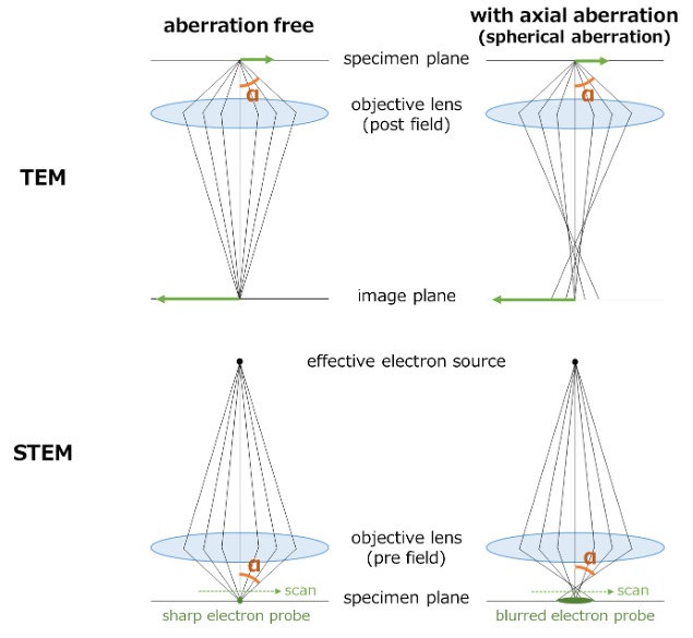
図1. TEM(上)およびSTEM(下)における軸上幾何収差のある場合とない場合。対物レンズに収差がない場合(左)と軸上収差(球面収差)がある場合(右)の光線図。TEMでは、収差があると試料の各点から出た電子が像面上で広がり、像がぼける。他方STEMでは、(仮想)光源から出た電子が試料面上で広がる。この像をプローブ(探針)として試料をスキャンして像を形成すると、像がぼける。
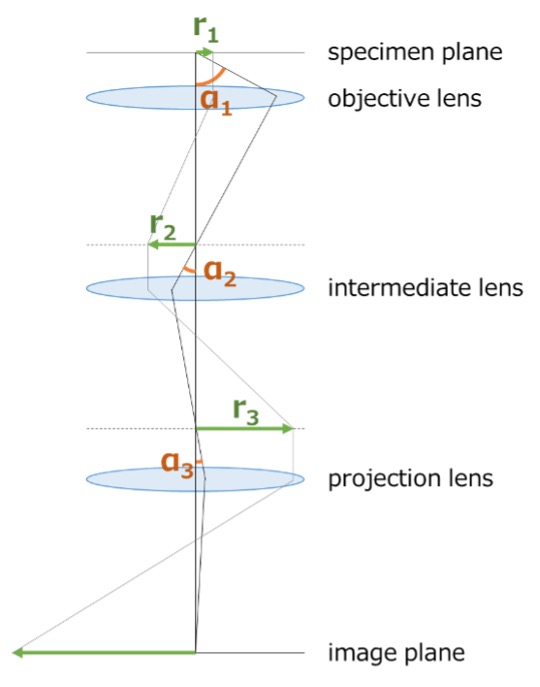
図2. 結像系の複数のレンズで像を拡大したときの、光軸からの距離rと光軸となす角αの変化。像が拡大されるほど、像の光軸からの距離が大きくなり(r1 < r2 < r3)、光軸となす角度は逆に小さくなる(α1 >α2 >α3)。軸上収差は光軸となす角度αのみに依存するため、より上方のレンズ(対物レンズ)の収差が像の劣化に影響する。
付録:軸上幾何収差と球面収差補正の進展
透過型電子顕微鏡では、対物レンズの球面収差(3次の軸対称収差)が長年、像の分解能を制限してきた。1980年代にはデフォーカス量を調整すること(シェルツァー・デフォーカス)によって、デフォーカスによる像のぼけと球面収差による像のぼけを相殺する方法が開発され、おおよそ10 mrad程度の角度範囲の電子線を用いることで高分解能像(~0.2 nm)が撮れるようになった。1990年代後半以降、6極子型および4極子8極子型の球面収差補正装置が実用化され、球面収差係数をゼロにできるようになった。球面収差補正装置では、軸上コマ収差や3回非点収差、スター収差、4回非点収差と呼ばれる寄生収差も補正でき、開き角α(半角)が大きい電子線(~30 mrad)を取り込んでも像面の一点に電子線を集光することができるようになった。球面収差補正装置の実用化により2000年代前半には像の分解能が0.1 nm以下になった。2000年代後半には電子顕微鏡自体の安定性の向上や冷陰極電解放出型電子銃の開発(光源の単色性の向上)により像の分解能が~0.05 nmに達した。
2000年代前半の6極子型球面収差補正装置での収差補正の角度範囲を30 mrad程度に制限していた原因は6回非点収差であったが、2000年代後半にはこの6回非点収差も補正できる収差補正装置(開き角~60 mrad)が実用化された。開き角が~40 mrad以上に取れるようになったことで、30~60 kVの低加速電圧で約0.1 nmの原子分解能を達成した。これによりグラフェンなど単原子層の観察が容易になった。また、焦点深度は開き角の2乗に反比例するので、開き角の増大は像の深さ方向の分解能を高めることにも貢献している。
The geometrical aberrations (departures of the path of electron beams from the path of ideal imaging on the image plane) are expressed as a function of r (distance of the electron beam from the optical axis) and α (opening angle between the electron beam and the optical axis). Among those aberrations, aberrations which depend only on the opening angle α, are called the axial geometrical aberrations (hereinafter, referred to be “axial aberrations”). It should be noted that, aberrations depending on r, and on both r and α, are called the off-axial geometrical aberrations (hereinafter, referred to be “off-axial aberrations”).
Table 1 lists the axial aberrations. The axial aberrations are classified by the order n of the opening angle α and the symmetry in the azimuth direction. For example, the first-order axially-symmetrical aberration is called “defocus” and the first-order two-fold symmetrical aberration is called “two-fold astigmatism.” The third-order axially-symmetrical aberration is called “spherical aberration”, which is well known as one of Five Seidel aberrations. Aberrations that are left blank in Table 1, such as the second-order two-fold symmetrical aberration, do not appear in principle.
When the axial aberrations exist, electron beams do not come to a single point on the image plane, but broaden to reduce the resolution of the image (Fig. 1). Among the many lenses of a transmission electron microscope (TEM), the aberration of the objective lens (post-field) has the greatest effect on the resolution of the image because the opening angle α is the greatest for the electron beam passing through the objective lens located closest to the specimen (Fig. 2). When observing the image of a specimen at a high magnification (high resolution electron microscopy), the observation area is small or the distance r is small. Thus, the off-axial aberrations can be ignored and only the axial aberrations of the objective lens are taken in account.
On the other hand, for obtaining a high-resolution image using scanning transmission electron microscopy (STEM), it is needed to converge the incident electron beam (incident probe) onto a specimen as smallest as possible. Thus, it is important to reduce the axial aberration of the condenser lens (actually the pre-field of the objective lens) located just in front of the specimen.
Table 1. List of axial geometrical aberrations. The aberrations are classified by giving the order n of the opening angle α in the vertical direction and the symmetry in the azimuthal direction in the horizontal direction. The blurring of the electron probe in STEM due to each aberration is shown.
Fig. 1. Ray paths through the objective lens with (right) and without (left) the axial geometrical aberrations in TEM (top) and STEM (bottom). In TEM, the aberration causes the electrons coming from each point of a specimen blurring on the image plane. In STEM, the aberration causes the electrons emitted from a (virtual) electron source a beam-broadening on the specimen plane. When an image is formed by scanning the specimen using the broadened beam (probe), the image is blurred.
Fig. 2. The increase of the distance r of the electron beam from the optical axis and the decrease of the opening angle α between the electron beam and the optical axis when an image is magnified by several lenses in the imaging system of the microscope. The more the image is magnified, the greater the distance r (r1 < r2 < r3), and to the contrary, the smaller the angle α (α1 > α2 > α3). Since the axial aberrations depend only on the opening angle α, the aberration in the upper lens (objective lens) has a crucial effect on degrading the image.
Appendix: The axial geometrical aberrations and advancement of correction of the aberrations
The spherical aberration of the objective lens (third-order axially-symmetrical aberration) had long been limiting the resolution of the image of the transmission electron microscope.
In the 1980s, a unique method was developed to cancel out the image blur caused by spherical aberration by adjusting the amount of defocus (Scherzer defocus) of the objective lens, which enabled us to take high-resolution images (~0.2 nm) using an electron beam with an angular range of approximately 10 mrad.
Since the late 1990s, spherical aberration correctors of the hexapole and quadrupole-octupole types have been put into practical use, enabling spherical aberration coefficients (Cs) to be reduced to zero. The spherical aberration corrector, Cs corrector, can correct not only the spherical aberration, but also the axial coma aberration and parasitic aberrations including the 3-fold astigmatism, star aberration, and 4-fold astigmatism. With this breakthrough, an electron beam can be converged onto a single point on the image plane even when an electron beam with a large opening angle α (semi-angle ~30 mrad) is accepted. In the early 2000s, practical use of the Cs corrector achieved the image resolution better than 0.1 nm. Furthermore in the late 2000s, the image resolution reached better than 0.05 nm owing to the improvement in the stability of the microscope and development of a cold field emission gun (which improved monochromaticity of the electron source).
In sextupole Cs correctors of the early 2000s, the angular range of aberration correction was limited to ~30 mrad by the six-fold astigmatism. But, in the late 2000s, aberration correctors (opening angle ~60 mrad) which can correct the six-fold astigmatism, put into practical use. By using an electron beam with an opening angle of ~40 mrad or better, an atomic resolution of about 0.1 nm was achieved at low acceleration voltages of 30 to 60 kV.
This facilitates to observe monoatomic layers such as graphene. It is important to note that the increase of the opening angle contributes to improve the resolution of the image in the depth direction because the focal depth is inversely proportional to the square of the opening angle.
関連用語から探す
説明に「軸上幾何収差」が含まれている用語


