タイコグラフィー
タイコグラフィー
Ptychography
[目次:理論(電子の散乱/回折/結像)]
入射電子プローブを、その照射領域の一部が重なるように試料上で二次元的に走査して各走査点において回折図形を取得し、一連の回折図形の強度から試料の構造を再構成する方法。Ptychoはギリシャ語で重なり (fold) を意味する。X線結晶構造解析の分野で実用的に使われている。
透過電子顕微鏡においては、装置の安定性向上と収差補正装置の開発とともに、回折図形の二次元デジタル画像を高速に取得できる高速高感度カメラの登場によって、より精度の高いデータ取得が可能となったことから、2012年頃から原子分解能の構造像を得る (位相回復) 手法の一つとしてタイコグラフィーが注目されてきた。特に近年の研究で、ノイズが少なくコントラストの高い結晶構造像 (図2) が得られることが報告され、関心を集めている。透過電子顕微鏡では、以下の二つの方法のタイコグラフィーが現在行われている。
1) 入射電子線を試料上でデフォーカスして照射した状態で走査する方法 (図 (a))
デフォーカスして照射領域を大きくした入射電子線を用いて、照射領域の一部が重なるように走査する。走査点数は、照射領域とプローブサイズに依存するが数10点×数10点以下である。タイコグラフィーにより結晶構造像 (位相回復像) を得る計算は以下のようにして行う。
デフォーカスして照射領域を大きくした入射電子線を用いて、照射領域の一部が重なるように走査する。走査点数は、照射領域とプローブサイズに依存するが数10点×数10点以下である。タイコグラフィーにより結晶構造像 (位相回復像) を得る計算は以下のようにして行う。
このようにして得られた試料の結晶構造像 (位相像) を図 (c) に示す。本手法は従来のインコヒーレントなディフラクティブイメージングと類似しているが、隣り合う照射領域の重なり部分で試料関数が一致することが拘束条件に加わっているために、ディフラクティブイメージングで起きている解の一意性の問題は克服されている。さらに観察領域も走査することによって制限されなくなっている。
2) 入射電子線を試料結晶上にフォーカスして照射した状態で走査する方法 (図 (b))
試料上にフォーカスした収束電子線を用いると、レンズの後焦点面にディスク上に広がった収束電子回折図形 (二次元図形) ができる。その収束電子線を試料上で二次元的に走査して (走査点は数万点を超える) 収束電子回折図形を取得すると、各入射方向に対する像、すなわち、(二次元走査像+二次元回折図形) の四次元データが得られる。
次に、[二次元走査像R+二次元回折図形K]の四次元データRKについて、二次元走査によって得られた像Rをフーリエ変換して回折斑点図形Qを得る。その結果、[二次元回折斑点図形Q+二次元回折図形K]の四次元データQKとなる。Qに含まれるある回折斑点 (反射) qを選んで、そのqに対する収束電子回折図形 (ディスク) Kと透過波ディスクとの干渉領域 (K') には、試料に対して弱位相物体近似が許される場合には、試料の結晶構造のフーリエ成分qに対する振幅と位相が表れている (図(b)下部)。引き続いて多くの回折斑点 (反射) qに対して、収束電子回折図形の重なり部分 (図(b) 下部K' とK'') から、それらの反射の振幅と位相を得る。得られた振幅と位相を反映させた二次元回折図形Q'を逆フーリエ変換して、試料結晶の構造像 (位相像) を得る (図 (d))。この方法を適用することによって、ADF像よりS/Nおよびコントラストの改善が見込まれる[2]。
その際、透過波に対して対称に位置する回折波 (-q) と透過波との干渉領域 (K'') の振幅の符号 (位相) を反転させ、干渉領域 (K') の振幅と同位相にする。(この操作によって、積分時に通常はK'とK''で相殺されてしてしまう信号を足し合わせて強度を増強できる。) さらに、得られる構造像 (位相像) のS/N比を改善するために、干渉領域 (K'、K'') の外の強度の振幅をゼロにする。
この手法は、原理的には結晶に限らず、非晶質にも適用できるとされている[3]。
(校閲 Associate Professor Peng Wang, University of Warwick)
文献:
[1]A. M. Maiden and J. M. Rodenberg: Ultramicroscopy, 109 (2009) 1256
[2]T. J. Pennycook et al.: Ultramicroscopy, 151 (2015) 160
[3]C. M. O’Leary et al.: Ultramicroscopy, 221, (2021) 113189
⇒図1
(a) 電子線の照射領域の一部が重なるようにして走査するタイコグラフィー。照射領域は数 nm~数10 nm程度で、走査点数は通常、数10点 ×数10点以下である。
(b) 電子プローブ (0.3 nm程度以下) を試料上にフォーカスして走査するタイコグラフィー。走査点数は通常のSTEMと同様に数100点 × 数100点程度。回折図形の取得には、高速高感度カメラ (ピクセル型STEM検出器) が用いられている。
(c) (a)の手法により再構成した単層MoS2の位相像 (構造像)。(データ提供:Associate Professor Peng Wang, University of Warwick)
(d) (b)の手法により再構成した単層グラフェンの位相像 (構造像)。
⇒図2
インフォーカスのタイコグラフィー再構成によって得られた構造像 (位相像)、および同時に取得されたADF像との比較。試料:単層グラフェン、加速電圧:80 kV
(a) 四次元データより再構成されたグラフェンの構造像。ここでは原子位置を明るく表示している。
(b) 四次元データと同時取得された通常のADF像。
両者を比較すると、再構成された構造像の方が、像のS/Nおよびコントラストがともに高くなっているのが分かる。
Ptychography is a method to reconstruct the crystal structure (image) of a specimen from the diffraction patterns obtained from each point (area) scanned over a specimen using a convergent probe so that a part of the illuminated area overlaps. "Ptycho" means "fold" in Greek. This method has been used in X-ray crystal structural analysis.
Ptychography for Electron Microscopy has attracted attention as one of methods to obtain the crystal structural image (phase recovery) of atomic resolution since about 2012, owing to the advent of a high-speed and high-sensitivity camera that achieves fast acquisition of a two-dimensional (2D) digital image, together with improvement of microscope stability and advancement of the aberration corrector. In particular, it has been reported in recent electron ptychography studies that low-noise and high-contrast crystal structure images are obtained (Fig. 2), thus gaining increased attention. In transmission electron microscopy, the following two types of ptychography methods are being conducted.
1) Scanning Method Using a Defocused Incident Electron Beam on a Specimen Crystal (Fig. (a))
A specimen is illuminated with a defocused convergent electron probe to broaden the illumination area. The probe is scanned on the specimen so that the adjacent illumination areas are partially overlapped with each other. The scanning points of the probe are typically fewer than several tens × several tens, depending on the scanning area and probe size. The procedure to obtain a crystal structure image (phase image) by means of this type of ptychography is as follows:
The initial specimen function is assumed equal to unity, and the probe function is assumed to be a box function. The exit-wave function from the specimen (the product of the specimen function and probe function) is Fourier-transformed to obtain the diffraction pattern. The amplitudes of the calculated diffraction pattern are replaced by the square root of the experimentally measured intensities, the phases of the diffraction pattern being unchanged. The updated diffraction pattern is inverse Fourier transformed to obtain the real space image (structure image), which gives a new revised specimen function at that probe position. The probe function obtained is replaced with the correct (initially defined) function, and the above procedure is repeated. Then, the same calculation procedure is carried out at the next position. The entire sequence of the procedure is repeated until the difference between the calculated and experimental diffraction patterns becomes sufficiently small [1].
The resulting crystal structural image (phase recovered image) of the specimen is shown in Fig. (c). Although the present method is similar to conventional incoherent diffractive imaging, it should be noted that non-unique solution problem in diffractive imaging is overcome due to the additional constraint, in which the specimen function in the overlapping region of the adjacent illumination areas must be the same. Furthermore, the observation area is no longer limited, as it can be expanded through scanning.
2) Scanning Method Using a Focused Incident Electron Beam on a Specimen Crystal (Fig. (b))
When a convergent electron beam is focused onto the specimen surface, a convergent beam electron diffraction (CBED) pattern - a disk shape pattern - forms on the back focal plane of the objective lens. By scanning this focused electron beam two-dimensionally across the specimen (with the number of scanning points exceeding tens of thousands) and by acquiring CBED patterns at each point, a four-dimensional dataset is obtained that includes images for each incident direction, i.e., (2D scanning image + 2D diffraction pattern).
Next, for the four-dimensional dataset RK composed of [2D scanning image R + 2D diffraction pattern K], a Fourier transform is applied to the scanning image R to obtain a diffraction spot pattern Q. As a result, a new four-dimensional dataset QK is formed, consisting of [2D diffraction spot pattern Q + 2D diffraction pattern K]. By selecting a specific diffraction spot (reflection) q from Q, the interference region (K') between the CBED disk K corresponding to the spot q and the transmitted wave disk contains the amplitude and phase information of the Fourier component q of the crystal structure—assuming the weak phase object approximation holds for the present case (see the lower part of Fig. (b)).
Subsequently, for many diffraction spots (reflections) q, their amplitudes and phases are extracted from the overlapping regions of the CBED patterns (K' and K'' in the lower part of Fig. (b)). By applying the inverse Fourier transform to the modified 2D diffraction spot pattern Q', which reflects the obtained amplitudes and phases, a structural image (phase image) of the specimen crystal is reconstructed (Fig. (d)). This method is expected to improve signal-to-noise (S/N) ratio and contrast better than those obtained with ADF (annular dark-field) imaging [2].
It is noted that in this procedure, the sign (phase) of the amplitude of the interference region (K'') between the diffracted wave (−q), which is symmetrically positioned with respect to the transmitted wave, and the transmitted wave is inverted to the same phase of the amplitude in the interference region (K'). This operation enables the enhancement of signal intensity by adding signals that would normally cancel each other out during integration between regions K' and K''. Furthermore, to improve the signal-to-noise (S/N) ratio of the resulting structural image (phase image), the intensity outside the interference regions (K', K'') is set to zero.
It should be noted that the technique described here is considered to be applicable not only to crystalline materials but also to amorphous substances [3].
(Proofread by: Associate Professor Peng Wang, University of Warwick)
References:
[1]A. M. Maiden and J. M. Rodenberg: Ultramicroscopy, 109 (2009) 1256
[2]T. J. Pennycook et al.: Ultramicroscopy, 151 (2015) 160
[3]C. M. O’Leary et al.: Ultramicroscopy, 221 (2021) 113189
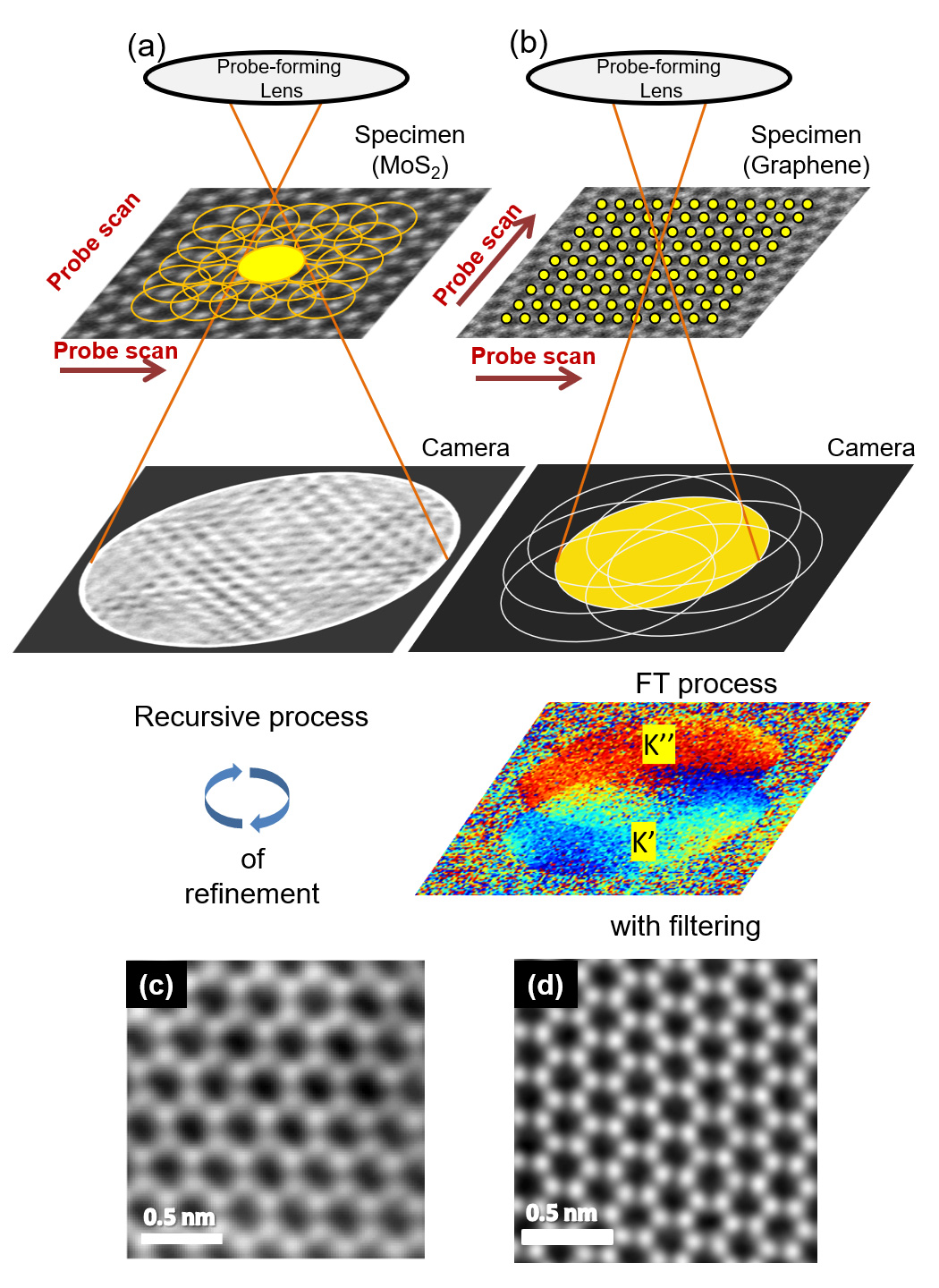
Fig. 1
(a) Ptychography in which a specimen is scanned with a defocused convergent electron probe so that adjacent illumination areas are partially overlapped to each other. The illumination area is about a few nm to a few 10 nm in diameter. The number of the scanning points is normally a few 10 times a few 10 or less.
(b) Ptychography in which a specimen is scanned with a focused convergent electron probe (probe diameter: about 0.3 nm or less). The number of the scanning points is a few 100 times a few 100 (the total number exceeding tens of thousands) like the case of ordinary STEM. A high-speed and high-sensitivity camera (pixel array STEM detector) is used to obtain a series of the CBED patterns.
(c) Structure image (Phase image) of a mono-layer of MoS2 reconstructed by the defocus method (a). (Data courtesy: Associate Professor Peng Wang, University of Warwick)
(d) Structure image (Phase image) of a mono-layer graphene reconstructed by the focus method (b).
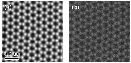
Fig. 2
Comparison of a reconstructed structure image (phase) obtained by Ptychography in which a specimen is scanned with a convergent probe and a simultaneously-obtained ADF image of a mono-layer graphene acquired at an accelerating voltage of 80 kV.
(a) Structure image (phase) of graphene reconstructed from 4D data set. Here, the atomic sites appear bright.
(b) Ordinal ADF image simultaneously acquired with the 4D data set.
Comparison of the two images elucidates that the reconstructed structure image (phase) has a higher signal-to-noise ratio and provides higher contrast than those of the ADF image.
関連用語から探す
説明に「タイコグラフィー」が含まれている用語


