双晶境界における角度差の精密測定
双晶境界における角度差の精密測定
Twin boundary-Precise measurement of angular difference
[目次:理論(電子の散乱/回折/結像)]
CBED法を用いると、双晶角 (双晶境界における結晶方位の角度変化) や、小傾角粒界における角度変化を、通常の制限視野電子回折の場合の精度約1°を、約2桁上回る0.01°程度の精度で求めることができる[1]。以下では双晶角測定についての例を述べる。
双晶角測定のためのdefocus CBED図形の撮影方法
図1に双晶角測定のためのdefocus CBED図形の撮影方法を模式的に示す。試料の表面に対して斜めに入っている双晶境界を考える。双晶境界より上側の結晶 (Domain 1) に対して、下側の結晶 (Domain 2) は角度δだけ結晶方位がずれているとする。コーン状の入射収束ビーム (入射コーン) の焦点を試料から上方にずらして (defocusして)、双晶境界を含む両側の領域を照射してCBED図形を撮影する (Defocus CBED法)。コンデンサー絞りの大きさで決まる回折ディスクを透過波と一つの回折波で示す。このとき、二つの結晶からの反射gの回折線 (の主極大) の位置が、図に示すように、ずれる。このずれは、 双晶境界での上下の結晶の方位変化に対応している。反射gの距離を基準として、このずれを測定することで、0.01°程度の高い精度で双晶角を求めることができる。
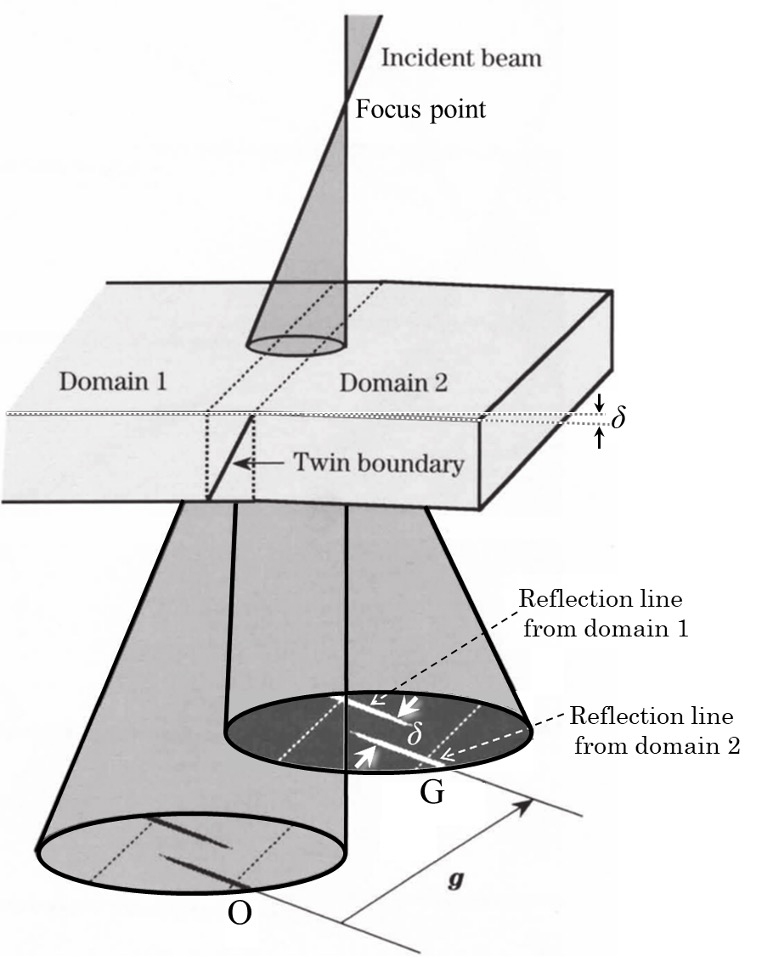
図1 双晶境界を含む領域から得られるdefocus CBED図形の模式図。
双晶境界をまたいでDomain 1とDomain 2からの回折線のずれが二つのディスク中に見られる。
ディスク中の点線は、双晶境界が試料の上面、下面と交わる線の投影を表す。
双晶による逆格子点のずれと回折線のずれ
高い精度で双晶角を決定するためには、双晶をなす二つのDomainの逆格子点のずれの方向が、電子線の入射コーンとほぼ平行になるように試料を配置しなければならない。図2 (a) に、Domain 1とDomain 2の逆格子点のずれを表すベクトル ∆gzと電子線の入射方向を模式的に示す。図中に、入射方向AおよびCに対応するエワルド球をそれぞれ実線で示した。また、Domain 1とDomain 2で反射gがBragg条件を満たす入射方向のエワルド球をそれぞれ点線で示した。図2 (b) に、この場合にDefocus CBED図形中に現れる回折線のずれの模式図を示す。透過ディスクOと回折ディスクG (およびG') の中に現れている回折線の間隔は反射gのブラッグ角の2倍2θBに対応し、2つの回折線のずれは双晶角δに対応する (δ = |∆gz|/|g|)。
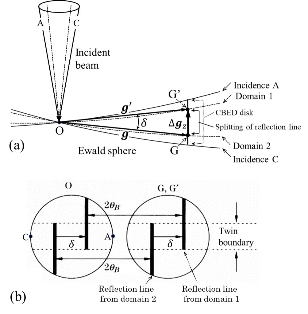
図2 (a) 双晶によるDomain 1の逆格子点GとDomain 2の逆格子点G'のずれと入射ビームに対するエワルド球の模式図。
結晶は、逆格子点のずれを表すベクトル∆gzが電子線の入射方向とほぼ平行になるように置かれている。
(b) 双晶によるDefocus CBED図形中の回折線のずれの模式図。
透過波ディスクOと回折ディスクG (およびG') の回折線間の距離は2θBに対応する。回折ディスク内の2つの回折線のずれは双晶角δに対応する (δ = |∆gz|/|g|)。
NiO (110) での双晶境界のdefocus CBED図形と双晶角の決定
図3に、NiOの (110) 双晶境界から加速電圧200 kVで得たdefocus CBED図形を示す。004, 006, 008反射の回折線が、図1に模式的に示したようにずれているのが分かる。双晶による回折線のずれ量は、同じ系列であればどの次数の反射でも同じになる。これは、双晶角は一つであり、反射の次数にはよらないためである。
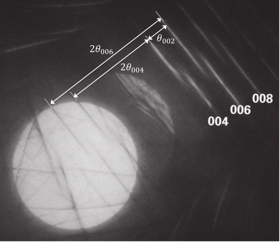
図3 NiOの双晶境界を含む領域から加速電圧200 kVで得たdefocus CBED図形。
2つのDomainからの004, 006, 008反射の回折線は同じ間隔でずれているのが分かる。
左下の明るい透過ディスク中にも004, 006, 008反射のずれが確認できる。
なお、この回折図形では、回折ディスクは互いに大きく重なるように設定されている。
図4は、NiOの (110) 双晶境界近傍から加速電圧200 kVで得た明視野defocus CBED図形 (大角度収束電子回折図形) および明視野TEM像である。双晶境界領域で00l系列の反射線のずれが見られる (矢印の対で示した)。ここで、004回折線と006回折線間の距離はブラッグ角θ002に対応する。(002) 反射の面間隔をdとして、ブラッグ反射の式 2d sin θB = λ を用いて、加速電圧200 kVでの004と006の回折線間の角度は θ002 = 0.344° と求められる。"2つのDomainからの004回折線のずれの距離"と"004と006回折線間の距離"の比は0.38と測定された。したがって2つのDomainからの004回折線のずれを角度に換算すると、0.344° × 0.38 ≈ 0.13° と求められた (この角度はDomain 1とDomain 2の (001) 面間の角度である)。この値を菱面体格子の角度αに直すとα = 90.07°となった。NiOは室温では菱面体相 (三方晶) に属し、格子定数はa = 4.177 Å、α = 90.06° と報告されている[2]。求めた値α = 90.07°は、報告されている値90.06°ときわめて良い一致を示している。
なお、(0k0) 面は両ドメインに共通な面なので、これらの面には角野の差はなく、したがって0k0系列の反射の回折線の分裂は見られない。
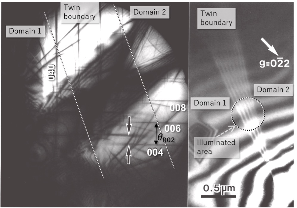
図4 NiOの双晶境界近傍から加速電圧200 kVで得た明視野defocus CBED図形 (大角度収束電子回折図形) および明視野TEM像。
TEM像のフリンジの部分が双晶境界である。 defocus CBED図形はTEM像中の点線で囲んだ領域から得た。
CBED図形中に矢印で示したように、双晶境界領域で00l系列の反射線のずれが見られる。
このように、二つのDomainからの逆格子点のずれの方向を入射電子線と平行にして方位の変化を測定すると、測定精度が0.01°まで飛躍的に向上する。一方で、逆格子点のずれの方向が入射電子線と垂直な場合には、角度測定の精度は制限視野電子回折の場合と同様の1°程度にとどまる。
なお、この方法は、双晶境界だけでなく小傾角結晶粒界に対しても同様に適用できる。
(東北大学教授 津田健治 執筆)
参考文献
- [1] M. Tanaka, M. Terauchi and T. Kaneyama, J Electron Microsc. 40, 211-220 (1991).
- [2] R. W. G. Wyckoff, Crystal Structures, Vol. 1, New York, Interscience (1963).
[付録] CBED図形で結晶の方位変化が高感度で観測できる理由
図5に、Domain 1の逆格子点を黒い丸、Domain 2の逆格子点を灰色の丸で示した。入射方向AおよびCに対応するエワルド球を図中に示した (簡単のためエワルド球は直線で近似)。逆格子点からのエワルド球までの距離を励起誤差と呼び、sで表す。エワルド球AおよびCで制限される領域が、回折ディスクの横方向の大きさに対応する。
回折ディスクgの直径は入射ビームの収束角2θに対応する。図5では、透過ディスクと回折ディスクgが接する条件になっており、入射ビームの収束角2θは2θBに等しい (θB: 回折波gの回折角)。
ディスク内に観測される双晶からの回折線は、双晶角δだけずれて観測される。このずれ量とディスクの直径との比はδ/(2θ) となる。入射ビームの収束角2θは加速電圧200 kVでは10 mrad (= 0.01 rad) 程度なので、δ/ (2θ)=δ×100となり、双晶での角度のずれδを100倍に拡大して見ていることになる。
これが、前述のNiOで高精度な角度変化が測定できる理由である。
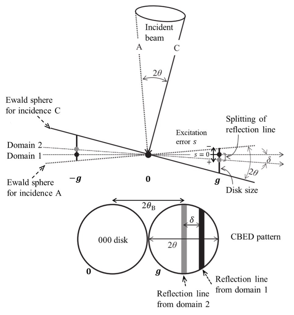
図5 CBEDディスク内の回折線と逆格子点の関係
Convergent-beam electron diffraction (CBED) enables us to determine the angular change at a twin boundary and angular difference at a small-angle grain boundary with a greatly high accuracy of 0.01°, which is two orders of magnitudes higher than the accuracy of 1° obtained by ordinary selected area diffraction (SAD) [1]. The measurement method is described using the twin angle of NiO as an example.
Method to acquire a defocus CBED pattern for measuring the twin angle
Fig. 1 illustrates the method to acquire a defocus CBED pattern to measure the angle of a twinned crystal. Let us consider the case of a twin boundary running oblique to the surface of a specimen. The crystal above the twin boundary (Domain 1) is assumed to have a different orientation from the crystal below the boundary (Domain 2) by an angle δ. By slightly defocusing the cone-shaped incident beam or by shifting the focal point of the beam a little upper from the specimen, the convergent beam is illuminated over an area of both domains across the twin boundary. This is called the defocus CBED method.
The size of the diffraction disks are determined by the size of the condenser aperture. The disk of the transmitted wave and the disk of a diffracted wave are shown. The diffraction lines (principal maxima) of the reflection g from the two domains are shifted, as shown in the figure. The shift corresponds to the change of crystal orientation between the domains above and below the twin boundary. From the ratio between this shift and the distance of the reflection g, the twin angle can be determined with an accuracy as high as 0.01°.
Fig. 1. Schematic of the defocus CBED pattern obtained from the area containing a twin boundary.
A shift is seen between the diffraction lines from Domain 1 and Domain 2 across the twin boundary, in the disks O and G.
The dotted lines in the disks are the projection of the intersecting lines of the twin boundary with the upper and lower surfaces of the specimen.
Shifts of reciprocal lattice points and diffraction lines from a twinned crystal
In order to determine the twin angle with a high accuracy, it is needed to set a specimen so that the shift direction of the reciprocal lattice points from the two domains is almost parallel to the incident electron beam.
Fig. 2 (a) depicts schematically a vector ∆gz representing a shift of the reciprocal lattice points for Domains 1 and 2, together with the direction of the incident electron beam. The Ewald spheres corresponding to incidence A and incidence C are shown by solid lines. The Ewald spheres corresponding to the incident beam directions where the reflection g satisfies the Bragg condition for Domain 1 and 2, are shown by dotted lines.
Fig. 2 (b) illustrates the shift of the diffraction lines appearing in the defocus CBED disks, corresponding to Fig. 2 (a). The distance between the diffraction lines in the transmission disk O and the diffraction disk G (or disk G') corresponds to 2θB, or twice the Bragg angle of the reflection g. The shift of the two diffraction lines in a disk corresponds to the twin angle δ (δ = |∆gz|/|g|).
Fig. 2 (a) Schematic of the shift between the reciprocal lattice points G of Domain 1 and G' of Domain 2 of the twins and schematic of the Ewald spheres for the incident beam cone.
The crystal is set so that the vector ∆gz representing the shift of the reciprocal lattice points is almost parallel to the incident beam direction.
(b) Schematic of the shift of the diffraction lines due to the two domains appearing in the defocus CBED patterns.
The distance between the two diffraction lines in the transmission disk O and the diffraction disk G (or disk G') corresponds to 2θB.
The shift of the two diffraction lines in each diffraction disk corresponds to the twin angle δ (δ = |∆gz|/|g|).
Defocus CBED pattern from a twin boundary of NiO (110) and determination of its twin angle
Fig. 3 shows a defocus CBED pattern of a twin boundary of NiO (110) taken at an accelerating voltage of 200 kV. The two diffraction lines in 004, 006 and 008 reflection disks are displaced as illustrated in Fig. 1. The displacement of the lines for each reflection is the same irrespective of the order of reflection. This is because the twin angle is constant independent from the reflection order.
Fig. 3. Defocus CBED pattern obtained from an area containing a twin boundary of NiO (110) taken at an accelerating voltage of 200 kV.
It is seen that the two diffraction lines from the two domains in the 004, 006 and 008 reflections are shifted with the same distance.
The shifts are also seen in the transmission disk at the lower left.
It is noted that in this pattern, the incidence beam angle is set to largely overlap the adjacent diffraction disks.
It should also be noted that the angle between the 004 and 006 diffraction lines does not correspond to 2θ002, but corresponds to θ002.
Fig. 4 shows a bright-field defocus CBED pattern (large-angle convergent-beam electron diffraction pattern) obtained from an area containing a twin boundary of NiO (110) at an accelerating voltage of 200 kV, together with a bright-field TEM image taken from the corresponding area. In the area of the twin boundary indicated by two dotted lines, the shift of the 004 reflection lines is seen (indicated by black arrow pairs).
The distance between the 004 and 006 diffraction lines corresponds to the Bragg angle θ002. Using Bragg's equation 2d sinθB = λ, the angle θ002 was determined to be 0.344° for 200 kV, where d is the distance of (002) lattice pane. The ratio of "the distance of the 004 diffraction lines from the two domains" to "the distance between the 004 and 006 diffraction lines" was measured to be 0.38. Then, the distance of the 004 diffraction lines from the two domains is converted to be an angle of 0.344° × 0.38 ≈ 0.13°. (This angle corresponds to the angle between the (001) planes of Domain 1 and Domain 2.) If this value is converted to the angle of the rhombohedral lattice α, the angle is determined to be α = 90.07°.
NiO belongs to the rhombohedral phase (trigonal crystal system) at room temperature, and the lattice constants are reported to be a = 4.177 Å, α = 90.06° [2]. The value obtained in the above experiment agrees very well with the reported value of 90.06°.
It is noted that the 0k0 reflections exhibit no splitting because the (0k0) planes are common for the both domains and have no angular change.
Fig. 4. Bright-field defocus CBED pattern (large-angle convergent-beam electron diffraction pattern) from an area containing a twin boundary of NiO at an accelerating voltage of 200 kV, together with a bright-field TEM image taken from the corresponding area.
The striped area in the TEM image corresponds to the twin boundary. The defocus CBED pattern was acquired from the area enclosed by a dotted circle in the TEM image.
A shift of the 004 reflections from the two domains is seen in the area of the twin boundary as indicated by the black arrows in the CBED pattern.
In summary, when the shift direction of the reciprocal lattice points from the two domains across a twin boundary is set parallel to the direction of the incident beam, the orientation change at the twin boundary can be measured with an accuracy of 0.01°, whereas when the shift direction is set vertical to the incident beam direction, measurement accuracy is only about 1°, as in the case of selected area diffraction.
It should be noted that this method can be applied also to the small-angle grain boundary.
(By Professor Kenji Tsuda, Tohoku University)
References
- [1] M. Tanaka, M. Terauchi and T. Kaneyama, J Electron Microsc. 40, 211-220 (1991).
- [2] R. W. G. Wyckoff, Crystal Structures, Vol. 1, New York, Interscience (1963).
Appendix. The reasons why the defocus CBED method can measure a change in crystal orientation with a high accuracy
Fig. 5 shows the reciprocal lattice points for Domain 1 as black points and those of Domain 2 as gray points. The Ewald spheres for the incident electron beam directions A and C are drawn by straight lines for simplicity, respectively with a dotted line and a solid line. The distance from the reciprocal lattice point to the Ewald sphere is called "excitation error" and this is expressed as s. The angle limited by the Ewald spheres A and C corresponds to the CBED disk size in the lateral direction.
The size or diameter of the diffraction disk g corresponds to the angle 2θ of the convergence angle of the incident beam in the present case. In Fig. 5, since the transmission disk contacts with the diffraction disk g, the convergence angle 2θ of the incident-beam is equal to 2θB. (θB: diffraction angle of the diffracted wave g )
The lines drawn with gray and black colors in the disk show the reflection lines from the Domains 1 and 2 of the twins with a shift of the twin angle δ.
The ratio of this shift to the disk diameter is δ/ (2θ). Since the convergence angle of the incident beam 2θ is approximately 10 mrad (= 0.01 rad) at an accelerating voltage of 200 kV, the shift can be expressed to be δ/ (2θ) = δ×100. This means that the angular difference δ at the twins can be observed to be magnified by a factor of about 100.
This advantage was demonstrated for a high-accuracy measurement of angular difference in the twin domains of NiO, described above.
Fig. 5. Relationship between the diffraction line in a CBED disk and the reciprocal lattice point
関連用語から探す
説明に「双晶境界における角度差の精密測定」が含まれている用語


