回折収差
回折収差
diffraction aberration, diffraction limit
[目次:理論]
電子の波動性によって起こる焦点面上での電子線の広がり。回折限界とも呼ばれる。
電子は波の性質を持っており、光と同様に回折現象 (波が物体の背後に回り込んで広がっていく現象) を起こす。SEMの対物レンズでは球面収差と色収差を小さくするために円形の対物絞りが使われる。この絞りの大きさが有限であるために起こる回折現象の結果、光軸と平行に対物レンズに入射する電子線はその焦点面上の1点に集束せず、光軸を中心とする円状の広がり (エアリー (Airy) ディスク) と、その回りにいくつかの円環 (エアリー (Airy) パターン) からなる干渉パターンになる。
図1に回折による電子プローブの焦点面上での強度分布を示す。エアリーディスクの強度が0になる半径 (暗環半径)  は、
は、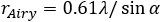 で表される。ここで、αは電子線の集束半角で、通常1~20 mradである。対物レンズと試料の間の距離 (working distance、WD) が短いとαは大きく、長いとαは小さい。λは電子の波長で、電子の加速電圧をVacc (V) とすると、
 (nm) と表される。焦点面での電子プローブの直径dd は近似的に第1暗環半径 に等しい。さらに、SEMでは通常αは20 mrad以下なので、sinを一次近似で計算して、
 ※1と書ける。
図2に回折収差による焦点面上での電子プローブ径の加速電圧変化を示す。加速電圧が低くなると、電子の波長λが長くなるため電子プローブ径が大きくなり、特に5 kV以下で回折の影響が顕著になる。例えば、α = 5.0 mradの場合、加速電圧20 kVでは dd = 1.1 nm であるが、加速電圧1 kVでは dd = 4.7 nm になる。
※1 L. Reimer, Scanning Electron Microscopy, Springer, Berlin, Germany, p. 27 (1998).
図1 電子の回折現象に起因する電子線の広がり
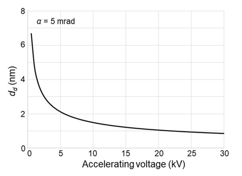
図2 電子プローブ径(dd)の加速電圧依存性 (α = 50 mrad)
The diffraction aberration causes a spread of an electron beam on the focal plane of the objective lens due to the wave nature of electrons. This term is also called "diffraction limit".
Electrons possess the wave nature and causes diffraction phenomena as light does. For the objective lens of the SEM, a circular objective aperture is used to decrease spherical and chromatic aberrations. Since the size of the aperture is finite, a diffraction phenomenon occurs. That is, the electron beam running parallel to the optical axis does not converge onto a point on the focal plane but forms an interference pattern, which is composed of a light disk around the optical axis (Airy disk) and plural circular rings (Airy pattern).
Fig. 1 shows the intensity distribution of the electron probe on the focal plane. The radius of the Airy disk () is expressed as . Here, α is the convergence semi-angle of the electron beam and usually 1 to 20 mrad. (If the distance between the objective lens and specimen (working distance, WD) is small, α becomes large, and vice vasa.) λ is the electron wave length. The wavelength is expressed as (nm), where Vacc is the accelerating voltage of the electrons. The electron probe diameter dd on the focal plane is approximated to be the radius of Airy disk or dd = . Since α for SEM is usually 20 mrad or less, sin α ≅ α and then .
Fig. 2 shows the accelerating voltage dependence of the electron probe diameter (dd) caused by diffraction. The electron probe diameter becomes large as the accelerating voltage becomes low or the electron wavelength λ becomes long. It is noted that the probe diameter rapidly increases below 5 kV. In the case of α = 5.0 mrad, dd is 1.1 nm for 20 kV, and dd is 4.7 nm for 1 kV.
Fig. 1 Schematic diagram of the spread of an electron beam on the focal plane due to diffraction.
Fig. 2 Accelerating voltage dependence of the electron probe diameter (dd)
関連用語から探す
説明に「回折収差」が含まれている用語


