後方散乱電子回折
後方散乱電子回折
electron backscatter diffraction, EBSD
[目次:理論]
図1に示すように、水平面に対して大きく傾斜させた(約70°)バルク結晶試料に電子プローブを照射し、試料からの後方散乱回折パターン(EBSDパターンあるいはEBSP, Electron Backscattering Pattern)から、電子プローブ照射点の結晶方位を測定する手法。
図1 EBSDパターン取得の概念図 ⇒ 図1
図2にEBSDパターンの形成の機構を模式的に示す。試料に入射した電子(i)は試料の原子で弾性散乱または非弾性散乱され、大きな角度範囲に散乱する(ii)。これらの電子のうちで、試料の結晶面に対してブラッグ条件 2d・sinθ=n・λ を満たす方向θに進んだ電子(iii)は回折されスクリーン上で回折斑点を作る。ここで、d:は格子面の間隔、θは、電子線が結晶面と成す角、n:は正の整数、λは電子波長を表す。ブラッグ条件を満たす電子線は一方向のみでなく、角度θを満たして円錐状(Φ方向)に広がる(iv)。その結果、回折斑点は線状の図形(v)になる。異なる方位の結晶面からの回折線が重なり、図3のような図形が得られる。これをEBSDパターンと呼ぶ(これは、従来から知られている菊池パターンと同じものである)。図3(a)はアルミナ、(b)は銅から得られたEBSDパターンである。
図2 EBSDパターンの形成の模式図 ⇒ 図2
結晶面(面間隔d)に対するブラッグ条件(2d・sinθ=n・λ)の角度θを満たして、且つ円錐状(Φ方向)に回折する電子線が回折線を作る。いろいろな方位にできる回折線の重ね合わせとしてEBSDパターンが形成される。
図3 EBSDパターン(a)アルミナ焼結体、(b)銅 ⇒ 図3
弾性散乱電子および非弾性散乱電子は入射電子の進行方向に近いほど強い強度分布を持つため、水平面に対する試料の傾斜角度が大きいほど(試料への入射電子の入射角度が小さいほど)EBSDパターンの強度が強くなる。試料の傾斜角度が小さくなり、入射電子の入射角度が40°以上になると、EBSDパターンの強度は急激に弱まる。このため試料を水平面に対して約70°傾け、入射角度を約20°にしてEBSDパターンを取得する。
EBSDパターンは、試料に対向する位置(電子線に対して約90°の位置)に置かれたスクリーンに投影される。投影されたEBSDパターンをCCDカメラまたはCMOSカメラでPCに取り込み、試料結晶の構造から得たシミュレーションパターンと比較して、電子プローブの照射点の結晶方位を決定する。したがって、EBSD法は、試料結晶の構造を既知と仮定しているので、結晶構造が分からない試料には適用できない。
方位測定ができる最小領域(空間分解能)は、Wフィラメントの熱電子銃SEMで約0.2 μm径、ショットキーエミッション型電子銃を搭載した高分解能SEMで10~20 nm径である。これらの値は、1 nA程度のプローブ電流を確保したときのプローブ径にほぼ等しい。また、EBSDパターンを作る試料の深さは、加速電圧や試料の原子番号に依存するが、試料表面からおよそ30~50 nmである。これ以上の深さに拡散した電子は、非弾性散乱によるエネルギー損失で波長が大きく変化してしまうため、パターンの形成に寄与しない。
電子プローブを試料表面のある領域で連続的に移動させながら、各測定点の結晶方位を表示することによって、結晶方位マップを自動的にかつ高速に得ることができる。連続測定の速度は、EBSDパターンの画質やその他の条件設定によるが、1秒間に60~3000点程度である。
EBSDシステムの開発メーカー各社は、試料結晶の配向に関する種々の情報を表示するアプリケーションソフトを充実させている。主要なものは、1) 逆極点図のカラーキーに従って、結晶粒ごとに結晶方位のカラーマップを表示する、2) 結晶粒界のみを表示する、3) 各測定点のEBSDパターンの鮮明さの違いを利用して、結晶性の良し悪しを明暗のコントラストで表示する、の3つである。
図4にネオジウム磁石(Nd2Fe14B)へのEBSDの応用例を示す。(a)はEBSD解析を行った試料位置の二次電子像である。(b)は結晶方位(逆極点図方位:Inverse Pole Figure, IPFともいう)マップで、右の逆極点図のカラーキーに従って表示している。試料に垂直な結晶面の方位が示されている。(c)は結晶粒界を示す像で、粒界が黒い線で示されている。連続する測定点での強度の差分(微分)像である。結晶粒内では方位がそろっているので、白色で示されている。(d)は IQ (Image Quality)マップと呼ばれる結晶性の良し悪しを示す像である。像中の明るい結晶粒は結晶性が良く(鮮明なEBSDパターンを示す)、明るさが減るにしたがって結晶粒の結晶性が悪くなることを表している。
図4 ネオジウム(Nd2Fe14B)磁石の測定例 ⇒ 図4
- 二次電子(SE, secondary electron)像。
- 結晶方位(IPF)マップ: 試料の結晶粒の方位のカラーマップ。カラーは右の逆極点図のカラーキーに従って表示した。
- 結晶粒界マップ: 隣り合う測定点での方位差が一定以上ある場所を黒色で表示したもの(差分像または微分像)で、結晶粒界が黒い線で示されている。なお、黒色で面積がある部分は非晶質と考えられる。
- IQ (Image Quality)マップ: 得られたEBSDパターンの鮮明さをパラメータとして結晶性の良否を表示したもの。結晶性が良い部分を明るく表示し、悪い部分を暗く表示している。黒色の部分はEBSDパターンが認識できなかった部分である。
測定結果ご提供: ネオジウム磁石(Nd2Fe14B)のEBSD測定例 JFEテクノリサーチ株式会社
A method to measure the local orientations of a crystalline specimen from an electron backscatter diffraction pattern (EBSD or EBSP), where a bulk specimen is largely tilted (about 70°) from the horizontal plane and is probed by the electron beam to acquire an EBSD pattern as shown in Fig. 1.
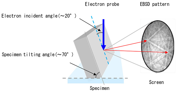
Fig. 1 Schematic of EBSD pattern acquisition
Fig. 2 shows schematically the formation of the EBSD pattern. The electrons incident onto the specimen (i) are elastically or inelastically scattered over a large angular range (ii) by the constituent atoms of the specimen. Among these electrons, the electrons travelling in a direction θ satisfying the Bragg condition (2d・sinθ=n・λ) with respect to the crystal lattice plane (iii) are diffracted and produce diffraction spots on the screen. Here, d is the spacing of the lattice plane, θ is the angle between the electron beam and the lattice plane, n is the positive integer and λ is the electron wavelength. The electrons travelling in different azimuthal directions φ with maintaining the Bragg condition (conical electron beams (iv)) also produce successive diffraction spots, forming a diffraction line (v). Many diffraction lines generated from the many lattice planes in different orientations are superposed and thus form an EBSD pattern. (This pattern is the same as the Kikuchi pattern already well known.) Fig. 3(a) and (b) show EBSD patterns obtained respectively from alumina (Al2O3) and from copper (Cu).
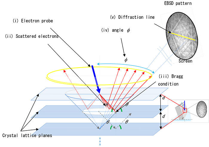
Fig. 2 Schematic of formation of EBSD pattern
The electrons which travel in the direction θ satisfying a Bragg condition (2d・sinθ=n・λ) with respect to the crystal lattice planes (lattice spacing: d) and in different azimuthal directions φ(conical electron beams), form a diffraction line. Superposition of many diffraction lines generated from many lattice planes with different orientations produces an EBSD pattern.
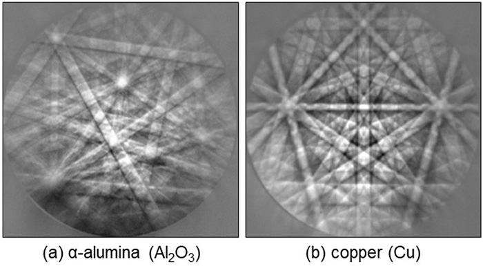
Fig. 3 EBSD patterns (a) α-alumina (Al2O3) (b) Copper (Cu)
Elastically and Inelastically scattered electrons closer to the incident electron beam direction have stronger intensity. Thus, for a larger specimen tilt angle with respect to the horizontal plane (for a small electron incident angle to the specimen), a higher intensity EBSD pattern is obtained. When the specimen tilt angle becomes small and the electron incident angle reaches 40° or more, the intensity of the EBSD pattern rapidly decreases. Thus, the EBSD pattern is acquired usually at a specimen tilt angle of about 70° to the horizontal plane or at an incident electron probe angle of approximately 20°.
The EBSD pattern is projected on a screen, which is placed against the tilted specimen and makes an angle of about 90° with respect to the optical axis of the electron beam. The projected EBSD pattern is stored in a PC using a CCD camera or a CMOS camera. Then, the EBSD pattern is compared with the simulated patterns computed based on the structure of the specimen. As a result, the crystal orientation at the electron-probe irradiation point is determined. Since the EBSD method assumes that the crystal structure of the specimen is known, the method cannot be applied to the specimen with an unknown crystal structure.
The smallest area (spatial resolution) of the crystal orientation measurement is approximately 0.2 μm in diameter for a thermionic-emission SEM equipped with a tungsten (W) filament and 10 to 20 nm in diameter for a high-resolution SEM equipped with a Schottky-emission electron gun. These values are almost equal to the electron-probe diameter when the probe current is approximately 1 nA. The specimen depth to generate the EBSD pattern ranges down to 30 to 50 nm from the specimen surface, though it depends on the accelerating voltage and the atomic numbers of the constituent elements in the specimen. The electrons scattered into deeper than this range suffer energy losses many time due to inelastic scattering, creating electrons with various wavelengths. Then, these electrons do not form the EBSD pattern.
An important feature of the EBSD method is crystal orientation mapping. That is, when the electron probe scans an arbitrary area of the specimen, the crystal orientations of each measurement point of the area are displayed and a crystal orientation map can be obtained automatically and rapidly. The speed of sequential measurement is approximately 60 to 3,000 points per second, though it depends on the image quality of the EBSD pattern and the image acquisition conditions.
Makers of developing EBSD systems provide a wealth of application software programs, which display a variety of information on the orientations of the crystalline specimen. Main application software programs include: 1) a program displaying a color map of the crystal orientations using color keys against the inverse pole figure (IPF). 2) a program displaying the grain boundaries. 3) a program displaying the crystal quality of each crystalline grain with a gray scale utilizing the difference in the sharpness of the EBSD pattern at each measurement point.
Fig. 4 shows an example of EBSD analysis applied to a neodymium magnet (Nd2Fe14B). Fig. 4(a) is a secondary electron image of a specimen position subjected to EBSD analysis. Fig. 4(b) is a crystal orientation map (also termed to be an inverse pole figure (IPF) map), which displays the orientations of the crystalline grains in the specimen using color keys in the figure to the right of (b). The orientations of the lattice planes vertical to the specimen surface are shown. Fig. 4(c) is an image showing crystalline grain boundaries with dark lines. This image is formed by intensity difference between successive measurement points (differential image). Since the crystal orientations are the same in the grains, the bodies of the grains are shown bright. Fig. 4(d) is an Image Quality (IQ) map displaying the quality of crystallinity. Bright crystal grains indicate to have high crystal quality (sharp EBSD patterns). Less bright grains indicate to have low crystal quality (smear EBSD patterns).
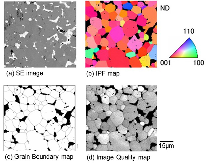
Fig. 4 EBSD analysis of a neodymium magnet (Nd2Fe14B).
- Secondary electron image.
- Crystal orientation (IPF: inverse pole figure) color map of the crystal grains in the specimen. Color keys for the IFP (the right of (b)) are used for the color presentation.
- Grain boundary map. The specimen positions at which the crystal orientation difference from the adjacent measurement points is larger than a certain angle, are displayed as dark (differential image map). Then, the crystalline grain boundaries are elucidated as dark lines. It is noted that the dark-color areas are regarded as amorphous regions.
- Image Quality (IQ) map. The crystal quality of the grains is displayed with a gray scale. The grains with a high crystal quality is shown bright and the grains with a low crystal quality is shown dark utilizing image sharpness of the acquired EBSD pattern. Black-color areas indicate the regions where EBSD patterns were not observed.
Data courtesy: The application example of EBSD analysis of a neodymium magnet (Nd2Fe14B) is supplied by the JFE Techno-Research Corporation
関連用語から探す
説明に「後方散乱電子回折」が含まれている用語


