コーティング
コーティング
coating, metal coating
[目次:試料作製]
コーティングとは、非導電性試料の表面にカーボンや金属の導電性薄膜 (厚さ数 nm - 10 nm程度) で覆うことである。入射電子 (試料に侵入する電子) が蓄積すると試料表面が負に帯電する。一方、試料から放出される二次電子が入射電子より多く放出されると正に帯電する。コーティングを行うことで、導電性薄膜を通して帯電した電荷をグラウンドへと逃すことができ、帯電による二次電子像の歪みや、試料の局所が極端に明るく (または暗く) なるといった像の異常を防ぐことができる。なお、試料に導電性がある場合はコーティングを行う必要はない。
図1に金 (Au) をコーティングした髪の毛と無処理の髪の毛をSEMで観察した例を示す。両者ともに同じ位置を観察している。Auをコーティングした髪の毛では導電性が得られ、表面の鱗模様を歪みなく観察できている (図1 (a) )。一方、無処理の状態では、帯電による入射電子線の偏向によって、髪の毛が実際の太さよりも細く見えている。また、帯電によって中央付近が異常に暗くなり、表面の鱗模様がよく見えなくなっている (図1 (b) )。
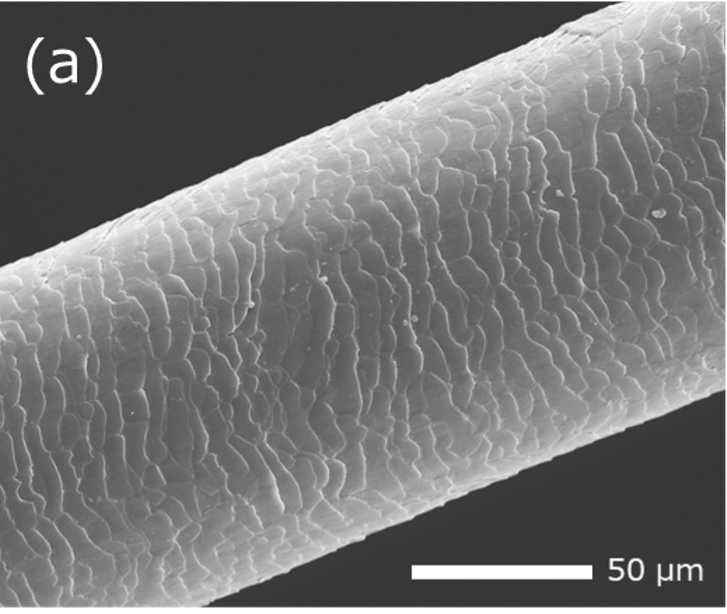
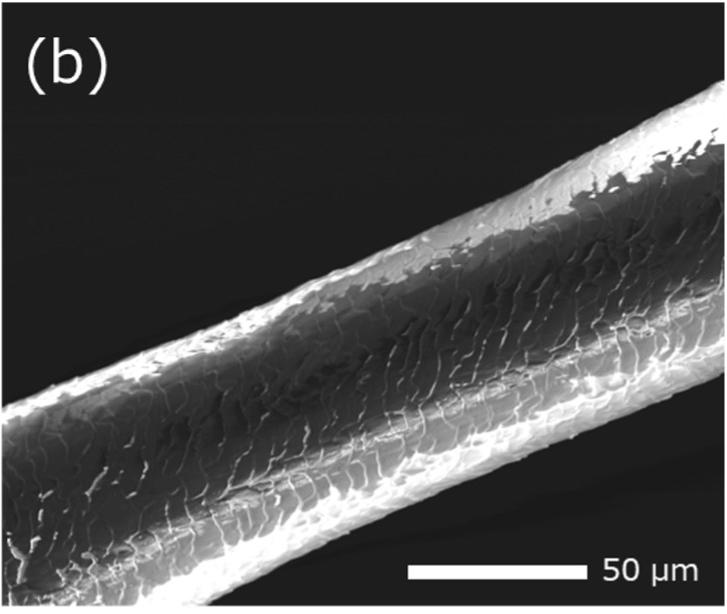
図1 コーティング有無の比較 (装置: JCM-7000, 加速電圧: 15 kV)
(a) 金 (Au) をコーティングした髪の毛の二次電子像。表面の鱗模様を歪みなく観察できている。Auの薄膜の厚さは数 nmのため、観察される形状に影響が出ない。
(b) 無処理の髪の毛の二次電子像。帯電による入射電子線の偏向により、髪の毛が実際の太さよりも細く見えている。また、帯電によって中央付近が極端に暗くなり、表面の鱗模様が不明瞭になっている。
表1 コーティング方法と材料
| コーティング方法 | 真空蒸着 | スパッタリング | プラズマ CVD | |
|---|---|---|---|---|
| 材料 | カーボン (C) | 金 (Au) | 白金 (Pt) | オスミウム (Os) |
| 粒の大きさ | SEMでは粒が見えない | 数十 nmの粒が見える | 数 nmの粒が見える | SEMでは粒が見えない |
| 試料に対する回り込みの良さ | 真空蒸着 (C) < スパッタリング (Au, Pt) < プラズマ CVD (Os) | |||
| 適する試料 | 元素分析を行う試料全般 | SEMで観察する試料全般 | 複雑な構造の試料 (多孔質材料、生物試料、繊維など) | |
| 観察や分析に使用できる倍率 (目安) | 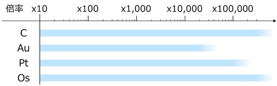 |
|||
表1 にコーティング方法と材料の特徴を示す。コーティング方法には真空蒸着、スパッタリング、プラズマCVD (化学気相成長) が用いられている。各コーティング方法で使用できるコーティング材料が異なる。真空蒸着ではカーボン (C)、スパッタリングでは金 (Au) や白金 (Pt)、プラズマCVDではオスミウム (Os) が用いられる。真空蒸着 < スパッタリング < プラズマCVDの順に、コーティング材料が試料の裏側まで回り込みやすくなる。
カーボンは元素分析に適している。その理由はカーボンのEDSスペクトルのKα線 (0.27 keV) が他元素由来のピークと重なりにくく、試料から発生した特性X線も吸収しにくいためである。一方、Au、Pt、Osは原子番号がそれぞれ79, 78, 76であり、EDSスペクトルのピークが互いに近い位置に出る。Au、Pt、OsのMα線 (1.9-2.4 keV) はリン (P) のKα線 (2.0 keV) や硫黄 (S) のKα線 (2.3 keV)、ジルコニウム (Zr) のLα線 (2.0 keV) と重複しやすいため、P、S、Zrを含む可能性のある試料の分析には、Au、Pt、Osをコーティング材として使用しない方が良い。
AuとPtを比較すると、Auの粒よりもPtの粒の方が小さいため、Ptを使用する方が良い。例として、無処理のカーボンブラック (煤の粒子) と、AuとPtをコーティングしたカーボンブラックをSEMで観察した結果を図2に示す。
無処理のカーボンブラック上に粒は見えない (図2 (a))。一方、Auをコーティングしたカーボンブラックでは、数十 nmのAuの粒が見えている (図2 (b))。Ptをコーティングしたカーボンブラックでは、Ptの粒はこの倍率では殆ど見えず、大きさは数nm程度と小さい (図2 (c))。
図2 (c) で見たようにPtをコーティングした場合は、高い倍率でも粒が見えにくいため、大きさが数 μm以下の試料 (例えば、ナノ粒子やレジストパターン、半導体の絶縁膜など) にも使用できる。さらに高倍率でSEM観察を行う場合には、より粒の小さいクロム (Cr) やイリジウム (Ir) をスパッタリングによりコーティングすることもある。
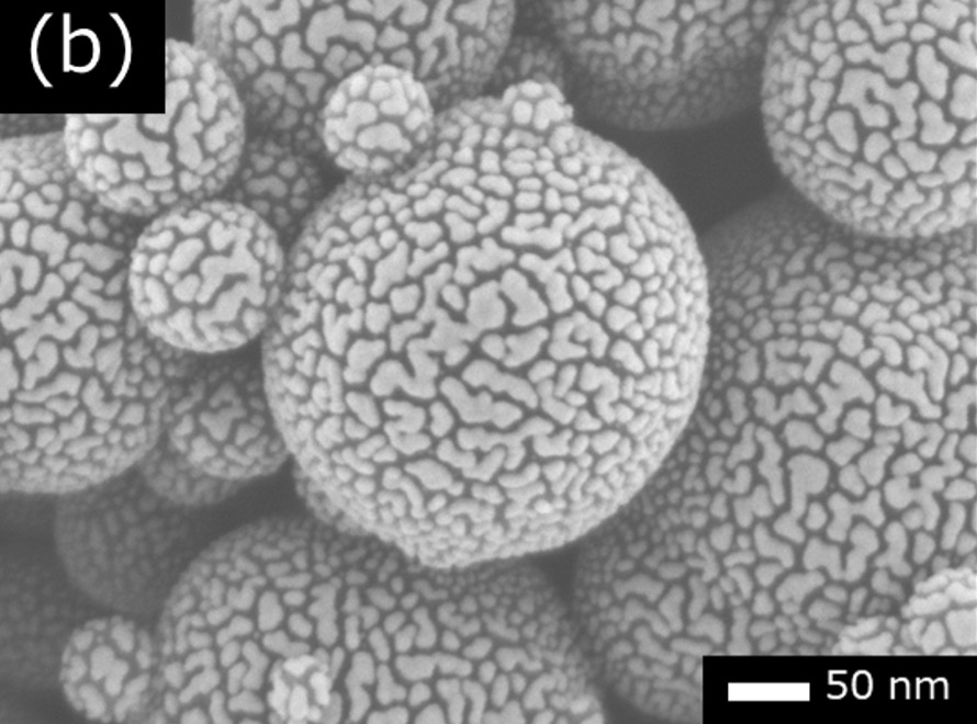
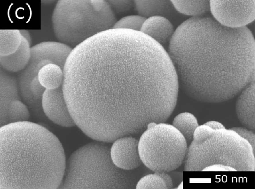
図2 金 (Au) と白金 (Pt) を用いたコーティングによる粒状性の比較
(装置: JSM-IT800SHL, 加速電圧: 1.5 kV)
(a) 無処理のカーボンブラックの二次電子像。カーボンブラックの表面に粒は見えない。
(b) Auをコーティングしたカーボンブラックの二次電子像。Auの粒の大きさは数十 nmである。
(c) Ptをコーティングしたカーボンブラックの二次電子像。Ptの粒の大きさは数 nmである。
四酸化オスミウム (OsO4) を用いたプラズマCVDは、試料の上面だけでなく側面や下面にも均一なコーティングが可能なため、複雑な構造を持つ多孔質材料や生物試料、繊維などの試料のコーティングに適する。ただし、OsO4が毒物であるため、取扱いに注意が必要である。OsO4のガスが外部に排出されないように、コーティング装置内にガスを吸収・除去するフィルターを設ける必要がある。
Coating is to cover the surface of a nonconductive specimen with a conductive thin-film (carbon or metal) of a few nm to 10 nm thick. If the incident electrons that enter a specimen are accumulated in a specimen, the specimen surface is negatively charged. If more secondary electrons are emitted from the specimen than the entering electrons, the specimen surface is positively charged.
When a conductive thin-film is coated, the extra electric charges escape to ground, and then distortion of the secondary electron image due to charging and image anomalies such as extremely light (or dark) images of local areas disappear. If the specimen is conductive, the coating is not needed.
Fig. 1 shows an example of SEM images taken from a human hair with gold (Au) coating and without coating. The Au-coated hair obtains conductivity and the scale patterns of the surface can be observed without image distortion (Fig. 1 (a)). On the other hand for the case of no coating, the hair is seen to be thinner than its actual thickness due to the deflection of the incident electron beam caused by charging. In addition, the charging causes the center region of the hair abnormally dark and the scale patterns of the hair surface cannot be seen clearly (Fig. 1 (b)).
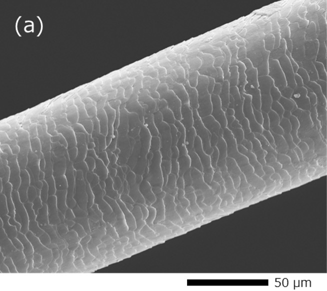
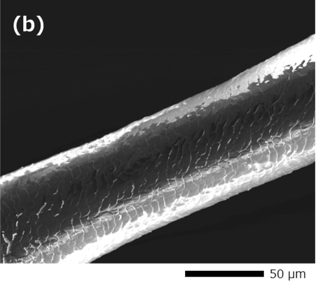
Fig. 1 Comparison of SEM images with and without coating.
(Instrument: JCM-7000, Accelerating voltage: 15 kV)
(a) Secondary electron image of a human hair with gold (Au) coating. The scale patterns of the surface are clearly seen without image distortion. It is noted that the Au film causes no effect on the observation of the morphology of the hair because of its thin thickness of only a few nm.
(b) Secondary electron image of a human hair without coating. The hair is seen to be thinner than its actual thickness due to the deflection of the incident electron beam caused by charging. The center region of the hair appears abnormally dark due to charging and the scale patterns of the hair become unclear.
Table 1 Coating methods and materials
| Coating method | Vacuum evaporation | Sputtering | Plasma CVD | |
|---|---|---|---|---|
| Material | Carbon (C) | Gold (Au) | Platinum (Pt) | Osmium (Os) |
| Particle | No particle is seen in a SEM image. | Particles (a few 10 nm size for a particle) are seen. | Particles (a few nm size for a particle) are seen. | No particle is seen in a SEM image. |
| Uniformity of coating | Vacuum evaporation (C) < Sputtering (Au, Pt) < Plasma CVD (Os) | |||
| Suitable specimen | All specimens for elemental analysis | All specimens for SEM observation | Complex-structure specimens (e.g. porous materials, biological specimens, fibers) | |
| Magnification range used for observation & analysis | 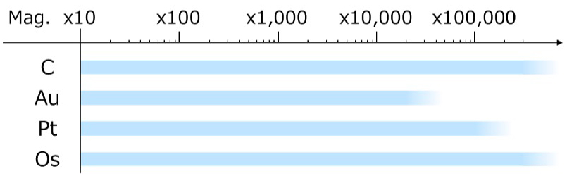 |
|||
Table 1 lists the coating methods and the characteristics of materials used for each coating. The coating methods used are vacuum evaporation, sputtering and plasma CVD (chemical vapor deposition). The coating materials available for each coating method are different; carbon (C) is used for vacuum evaporation, gold (Au) and platinum (Pt) for sputtering, and osmium (Os) for plasma CVD. The coating material is likely to reach and cover the backside surface of the specimen in the order of vacuum evaporation < sputtering < plasma CVD.
Carbon is suitable for elemental analysis. This is because the Kα line (0.27 keV) of the EDS spectrum of carbon hardly overlaps with the peaks originating from the other constituent elements of a specimen and carbon hardly absorbs characteristic X-rays generated from the specimen.
Au, Pt and Os, whose atomic numbers are respectively 79, 78 and 76, produce their EDS spectral peaks close to each other. It should be noted that the Mα lines (1.9 to 2.4 keV) of Au, Pt and Os overlap with the Kα line (2.0 keV) of phosphor (P), the Kα line (2.3 keV) of sulfur (S) and the Lα line (2.0 keV) of zirconium (Zr).
Thus, those coating materials are better not be used in the analysis of specimens that may contain P, S, and Zr.
Comparing Au and Pt, it is better to use Pt because Pt particles are smaller than Au particles. Fig. 2 shows a comparison example of SEM images of carbon black (soot particles) in three cases; without coating, with Au-coated and with Pt-coated. In Fig. 2(a), no metal particle is seen on carbon black. In Fig. 2(b), Au particles with a size of a few 10 nm are seen. In Fig. 2(c), Pt particles are hardly visible at this magnification and are only a few nm in size.
As seen in Fig. 2(c), since Pt particles are hard to be seen even at high magnifications, Pt coating can be used for specimens with a size of a few μm or less (e.g. nano-particles, resist patterns and insulating films of semiconductors). For even higher-magnification SEM observation, chromium (Cr) or iridium (Ir), which has a smaller particle size than Pt, can be coated by sputtering.
Fig. 2 Comparison of granularity with gold (Au) and platinum (Pt) coatings.
(Instrument: JSM-IT800SHL, Accelerating voltage: 1.5 kV)
(a) Secondary electron image of carbon black without coating. No particle is seen on the surface of carbon black.
(b) Secondary electron image of carbon black with Au-coated. The particle size of Au is a few 10 nm.
(c) Secondary electron image of carbon black with Pt-coated. The particle size of Pt is a few nm.
Plasma CVD using osmium tetroxide (OsO4) is suitable for complex-structure specimens such as porous materials, biological specimens and fibers, as it enables uniform coating for not only the top surface of a specimen but also the side and bottom surfaces. However, it should be noted that OsO4 is toxic and must be handled with special care. A filter must be set in the coating system to absorb and remove OsO4 gas to prevent the leakage of the gas to outside.
関連用語から探す
説明に「コーティング」が含まれている用語


