集束イオンビーム装置
集束イオンビーム装置
focused ion beam system, FIB system
[目次:試料作製]
集束イオンビーム装置 (FIB装置) とは、イオンビームを利用し、試料を観察して加工を行う装置である。試料表面を観察し、試料上の特定の位置に対して局所的な加工や成膜 (デポジション) を行う。走査電子顕微鏡 (SEM)、透過電子顕微鏡 (TEM) 用の試料作製や、半導体デバイスの回路修正、金属、ソフトマテリアル、固定化させた生物試料などの微細形状加工に用いられる。
FIB装置の基本機能は (1) 観察、(2) 加工、(3) デポジションの3つである。
(1) 観察 : イオンビームを試料に照射し、放出された二次電子を検出することでSIM像 (Scanning Ion Microscope像) が得られる。SIM像は走査電子顕微鏡像 (SEM像) に比べて、組成や結晶方位に敏感である。
(2) 加工 : 試料に照射されたイオンビームは試料内に進入し、試料を構成する原子をはじき出す (スパッタリング)。試料に対してイオンビームを走査することで、特定範囲の加工を行うことができる。
(3) デポジション : ガスインジェクション装置から有機ガスを試料表面に吹き付けながらイオンビームを照射することで、二次電子と有機ガスが反応し局所的に膜の形成を行う機能である。ガス源には、おもにカーボン化合物 (C14H10)、タングステン化合物 (W(CO)6)、プラチナ化合物 ((CH3C5H4)(CH3)3Pt) を用いる。ガス源に含まれるカーボン (C) はおもに試料表面の保護、タングステン (W) は半導体デバイスの配線作製、プラチナ (Pt) はその両方に使用される。
FIB装置の基本構成を図1に示す。イオン源、イオン光学系、二次電子検出器、ガスインジェクション装置、試料ステージ、真空排気系、制御系から構成される。イオン源には液体金属イオン源 (Liquid Metal Ion Source: LMIS)、ガスイオン源 (Gas Field Ion Source: GFIS)、プラズマイオン源などが使用される。最も一般的に用いられるのはLMISである。LMISのイオン材料としてはガリウム (Ga) が主流である。Gaは融点が常温に近く (29.7°C)、蒸気圧が低い (10⁻6 Pa以下) ため真空内でも蒸発によるGaの消耗が起こらない。また、針材料であるタングステン (W) と反応せず、かつ濡れ性が良い特徴がある。
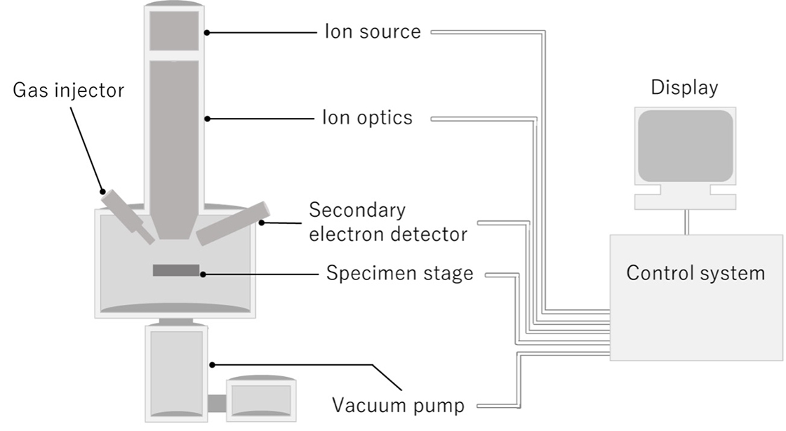
図1. FIB装置の基本構成
図2は、LMISの構造図である。イオンビームの材料である金属 (通常Ga) をフィラメントで一時的に加熱することで、貯蔵部内の金属 (Ga) が溶解してW針の先端が濡れる。針先端の液体金属は表面張力によって丸くなるが、引出電極にマイナス数 kVの電圧を印加することで針先端に強電界が形成され、液体金属が引っ張られて円錐形状になる (Taylor cone)。円錐先端にはさらに電界が集中し、イオン化した金属が放出される。
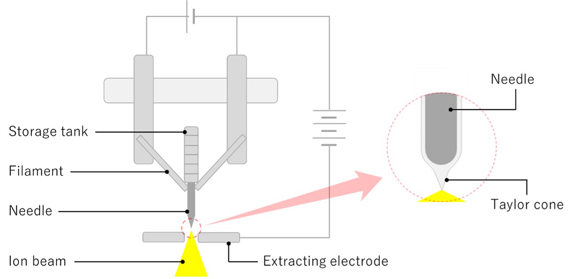
図2. 液体金属イオン源 (LMIS) の構造
図3にイオン光学系の構造を示す。イオン源から放出されたイオンビームは、2段の静電レンズにより試料上に集束される。すなわち、イオンビームはイオン源の直下に位置するコンデンサーレンズと絞りによって電流量が数十 nA~数 pA以下の範囲で制御され、さらに絞りを通過して対物レンズの作用を受けて試料上に集束される。集束されたイオンビームは、偏向電極により試料上を走査し、試料の観察、加工、およびデポジションを行う。数十nAの大電流のイオンビームは数百 µmの大領域を加工する際に使用され、数 pAの微小な電流のビームは数 nmオーダーの微細加工に使用される。
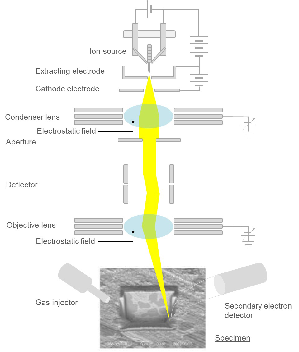
図3. FIB光学系の構造
A focused ion beam system (FIB system) is an instrument to observe and mill a specimen using an ion beam. That is, while observing the specimen surface, local milling and deposition of specific areas of the specimen are performed. The system is applied to specimen preparation for scanning electron microscopy (SEM) and for transmission electron microscopy (TEM), and circuit modification of semiconductor devices, and micro-shape processing of metals, soft materials and biological specimens subjected to fixation.
The basic functions of the FIB system are (1) observation, (2) milling and (3) deposition of the specimen.
(1) Observation: An ion beam is irradiated onto a specimen surface. Using the secondary electrons emitted from the specimen, a Scanning Ion Microscope (SIM) image is observed. The SIM image is more sensitive to the composition and the crystal orientation of the specimen than the Scanning Electron Microscope (SEM) image.
(2) Milling: The ion beam irradiated onto the specimen enters the specimen and sputters the constituent atoms of the specimen (sputtering). By scanning the ion beam onto the specimen, milling of the specific areas is performed.
(3) Deposition: By irradiating an ion beam while spraying organic gas from a gas injector onto the specimen surface, the secondary electrons react with the organic gas to form a local deposition of a film.
The gas sources are mainly carbon compounds (C14H10), tungsten compounds (W(CO)6) and platinum compounds ((CH3C5H4)(CH3)3Pt). Carbon (C) in the gas source is mainly used to protect the specimen surface, tungsten (W) is used to fabricate wiring for semiconductor devices, and platinum (Pt) is used for both applications.
Fig. 1 shows the basic construction of the FIB system. The system is composed of an ion source, ion optical system, secondary electron detector, gas injector, specimen stage, vacuum evacuation system and control system. For the ion source, a liquid metal ion source (LMIS), a gas field ion source (GFIS), or a plasma ion source is used. Among them, LMIS is most-widely used. Gallium (Ga) is the most commonly used ion material for LMIS, because its melting point is close to room temperature (29.7 °C) and its vapor pressure is low (less than 10-6 Pa), which prevents Ga from being consumed by evaporation even in a vacuum. In addition, Ga does not react with tungsten (W), a needle material, and has good wettability.
Fig. 1. FIB-system
Fig. 2 illustrates the construction of the LMIS. By temporarily heating the metal (usually Ga) of the ion source with a filament, the Ga metal in the storage tank melts and wets the tip of the W needle. The liquid Ga at the tip of the needle becomes round by surface tension. When a negative voltage of a few kV is applied to the extracting electrode, a strong electric field is formed at the tip of the needle, and the liquid Ga is attracted by the electric field to form a cone shape (Taylor cone). The electric field is further concentrated at the tip of the cone, and the ionized Ga is emitted.
Fig. 2. Liquid metal ion source (LIMIS) system
Fig. 3 illustrates the ion optical system. The ion beam emitted from the ion source is focused onto the specimen by a two-stage electrostatic lens. That is, the electric current of the ion beam is controlled within several 10 nA to several pA by the condenser lens and the aperture located directly below the ion source, and then, the ion beam passes through the aperture and is focused on the specimen by the objective lens. The focused ion beam is scanned over the specimen by using the deflector electrode, for observation, milling and deposition of the specimen. A high-current ion beam of several 10 nA is used for milling a large area of several 100 µm, while a low-current beam of several pA is used for fine milling of an area of the order of several nm.
Fig. 3. FIB ion optical system.
説明に「集束イオンビーム装置」が含まれている用語


