シリコンドリフト検出器
シリコンドリフト検出器
silicon-drift detector, SDD
[目次:分析]
シリコン単結晶に、円盤状のカソード、環状電極と小さな収集電極 (アノード) を備えたエネルギー分散型X線分光 (EDS, Energy Dispersive X-ray Spectroscopy) 用の検出器(SDD, Silicon-drift detector)。
電子顕微鏡に搭載し、電子線を試料に照射した際に発生する特性X線を検出することで元素を同定する。従来のSi (Li) 型検出器に比べ、電気信号の高速処理が可能になり、計数率が2桁以上 (>105cps) 向上した。その結果、元素分析のスピードが向上した。
液体窒素冷却でなくペルチェ冷却で作動するため検出器は小型軽量になり、現在はEDS検出器の主流になっている。エネルギー分解能はSDDが128-135 eV (Mn Kα線 (5.9 keV)) で、Si (Li) 型検出器の130-140 eVより向上している。
SDDおよびSi (Li) 型検出器ではともに、X線が検出器のシリコン単結晶に入射すると電子-正孔対が発生し、電子 (電荷Q) はアノードへ移動し、正孔はカソードに移動する。その結果、カソードとアノードの間に電圧Vを生じる。その電圧を測定することから、最終的に構成元素を同定している。
Si (Li) 型検出器では、アノードの面積がX線の受光面と同じ面積で静電容量Cが大きく、ノイズN に対する信号S (∝電圧V、V=Q/C) の割合が十分でなかった。そのため、ノイズの主要因である熱ノイズを減らすためにシリコン単結晶を液体窒素で冷却し、さらに、信号を長時間積算することでノイズNの割合を減少させ、S/N比を向上させる必要があった。
そのため、受光面が10 mm2より大きなSi (Li) 型検出器ではS/N比をあげるために、長時間の信号積算が必要で実用的ではなかった。
他方、SDDでは、静電容量を小さくするため、図1のように、受光面 i の反対側の中心に10-4 mm2 (幅10 µm 程度) 以下の小さなアノード ii を配置し、その周りに環状電極 iii が置かれている。環状電極には、発生した電子をアノードに集めるために、外側から内側に行くにしたがって電圧が段階的に高くなるようにしてある。
このアノードとカソードの間で作られる静電容量Cが小さいため信号Sが大きくなり、液体窒素ではなくペルチェ冷却 (-数10℃程度) および短い積算時間で高いS/N比が得られる。その結果、特性X線の計数率がSi (Li) 型検出器に比べ、2桁以上(>105cps)向上し、短時間での特性X線の測定ができるようになった。
さらなる計数率向上のため、受光面を大きくしても、高いS/N比を保つことができるので、信号の積算時間は短くてすむ。現在は、受光面が100 mm2を超える検出器も実現している。計数率の向上により、元素分析のスピードが向上したことで、SEMの照射電流を大きくし、SEM像観察と同時に元素分析を行うリアルタイム分析やライブ元素マッピングが可能になっている。
また、X線の発生量が少ない低加速電圧での分析が広く行われるようになった。
SDDの動作原理
特性X線がSDDに入射し、元素が同定されるまでの動作を図1に示す。
カソードi には負の電位、アノードii には正の電位を印加する。環状電極iii には、電子がアノードii に向かうような負の電位を与える。特性X線のエネルギーを hν (h プランク定数、ν 振動数) とすると、このエネルギーに比例した数の電子-正孔対がシリコン単結晶内に発生する。
1対の電子-正孔対の生成エネルギーが3.6eVなので、例えば、Mn Kα線(5.9keV)の1光子は、電子-正孔対を約1600対発生させる。発生した電子-正孔対のうち電子は、環状電極iiiおよびアノードii に向かう。環状電極に到達した電子は、環状電極とアノードの間にかけられた電位勾配によって、アノードに集められる。
正孔はカソードi に移動する。カソードi とアノードii の間には静電容量Cがあり、コンデンサーを形成している。コンデンサーに生じた電圧Vを測定する。その電圧VからV=Q/Cという関係を使って電荷Qがわかり、電子1個の電荷量で割れば、発生した電子の個数がわかる。電子の個数からX線のエネルギーを得ることができる。
その結果、最終的に、元素が同定される。実際には、電圧VとX線のエネルギーとの関係は、標準試料を用いて校正する。
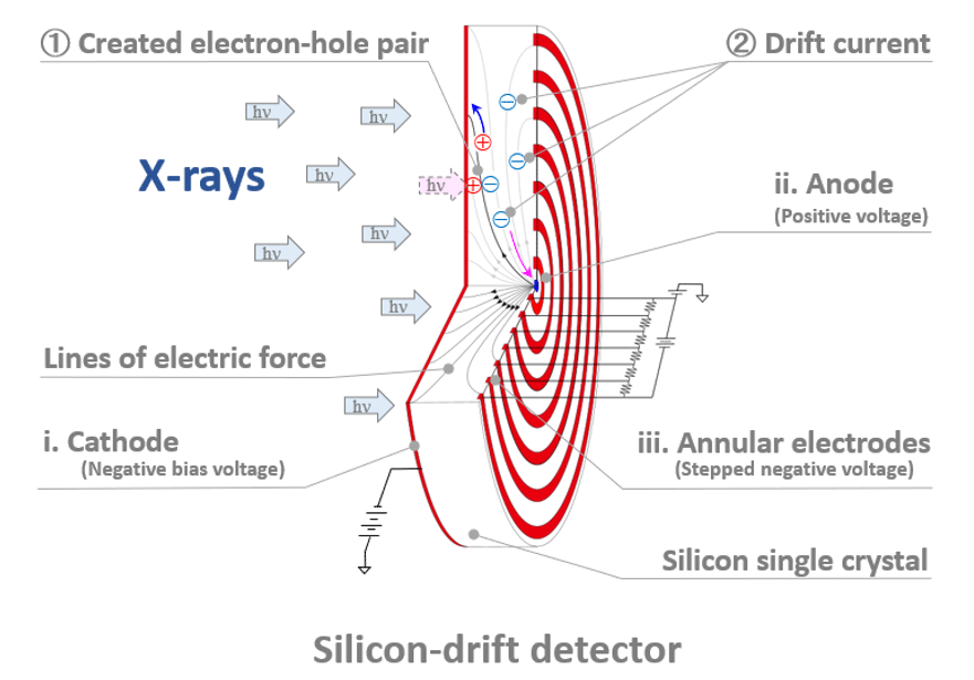
図1. 特性X線が左からシリコン単結晶に入射する。
①正孔-電子対が生成される。
②カソードi とアノードii および環状電極iiiの間にかけられた電位差により、電子はアノードii と環状電極iii に向かう。環状電極に到達した電子は、環状電極とアノードの間にかけられた電位勾配によって、アノードに集められる。正孔はカソードi に移動する。集積した電荷Qによりカソードi とアノードiiの間に作られたコンデンサーに発生する電圧Vを測定する。
この電圧Vから集積した電荷QがV=Q/Cの関係から分かり、特性X線1光子あたりに発生した電子数を求め、特性X線のエネルギーを算出することで、最終的に元素が同定される。
The silicon-drift detector (SDD) is an EDS (energy dispersive X-ray spectroscopy) detector, which is composed of a detector element made of a silicon (Si) single crystal, a disc-shaped cathode, annular electrodes and a very small collector electrode (anode).
The detector is attached to an electron microscope and is used to identify constituent elements in a specimen by detecting the characteristic X-rays generated from the specimen with electron-beam irradiation onto it. Compared with the conventional Si(Li) detector (SSD), the SDD has enabled high-speed processing of electric signals and has achieved a high count rate of more than two orders of magnitudes (>105 cps). As a result, analysis speed of the constituent elements has become much faster than that of the SSD.
Furthermore, since the SDD is operated with Peltier cooling (not with liquid-nitrogen cooling), the detector is compact and light-weighted. Now the SDD is the mainstream of EDS detectors. The energy resolution of the SDD (128 to 135 eV for Mn Kα (5.9 eV)) is a little better than that of the Si(Li) detector (130 to 140 eV).
The measurement principle of the SDD and the Si(Li) detector is the same. That is, when characteristic X-rays are incident onto a Si single crystal, electron-hole pairs are generated. Electrons (charge Q) move to the anode and holes move to the cathode.
Then, a voltage V is generated between the cathode and the anode. By measuring the voltage, finally the constituent elements are identified.
In the Si(Li) detector, since the anode size is the same as that of the incident plane (cathode) of the X-rays, the capacitance C of the detector (condenser) is large. Thus, the ratio of the signal S (∝voltage V, V= Q/C) to the noise N (S/N ratio) is low. To improve the S/N ratio, thermal noise (main noise) has to be reduced by cooling the detector with liquid nitrogen and by a long signal acquisition time.
Thus, it is not practical to use a large Si(Li) detector with a size of 10 mm2 or more, because it requires a very long signal-acquisition time for improving the S/N ratio.
In the SDD, in order to decrease the capacitance C of the detector, the electrodes have a unique structure as shown in Fig. 1. A very small anode (ii) of 10-4 mm2 (width of ~10 µm) or less is placed at the center on the opposite side of the incident plane (cathode (i)), and the annular electrodes (iii) are surrounding the anode (ii). The electrons that reach the annular electrodes (iii) are collected to the anode by applying the voltage which increases stepwise from the outside to the inside to the annular electrodes.
Then, the capacitance C of the detector becomes small and the signal S becomes large. As a result, a sufficient S/N ratio is obtained even by Peltier cooling (about –several 10 °C) and even by a short signal acquisition time. The count rate of characteristic X-rays has greatly improved, more than two orders of magnitudes (>105 cps) compared with the Si(Li) detector. Finally, short-time elemental analysis is achieved. Furthermore, a large size detector can be manufactured for further improvement of the count rate because the SDD can maintain a high S/N ratio irrespective of the incident plane size thanks to the small anode. Nowadays, an SDD with an incident plane of 100 mm2 or more is developed for practical use.
Owing to the high speed of elemental analysis, SEM image observation with real-time elemental analysis or live elemental mapping is now being possible using a large probe current. Elemental analysis at low accelerating voltages using the SDD has also become possible at which the generation of characteristic X-rays is small.
Action of SDD
Fig. 1 shows the action of the SDD until characteristic X-rays enter the detector and finally the constituent elements are identified.
A negative potential is applied to the cathode (i) and a positive potential is to the anode (ii). Negative potentials to increase stepwise from the outside to the inside are applied to the annular electrodes (iii) so that the electrons reached them are collected to the anode (ii).
When the characteristic X-ray with an energy of hν (h: Planck’s constant, ν: frequency of the X-ray) is incident on Si, electron-hole pairs are generated in proportion to the X-ray energy. Since the energy needed to generate one electron-hole pair is 3.6 eV, one photon of Mn Kα (5.9 keV) creates approximately 1600 electron-hole pairs. The electrons in those electron-hole pairs move to both the anode (ii) and the annular electrodes (iii). The electrons which reached the annular electrodes are collected to the anode by the stepwise potential. On the other hand, the holes move to the cathode (i). A condenser with capacitance C is formed between the cathode (i) and the anode (ii). The voltage V across the condenser is measured. Then, the electric charge Q accumulated in the condenser is obtained using the relation V = Q/C. The number of the generated electrons is calculated by dividing the charge Q by the charge of one electron. Then, the energy of the characteristic X-ray is obtained from the number of the electrons generated by one photon. Finally, the constituent element is identified from the obtained X-ray energy. In the actual measurement, the X-ray energy is obtained from the measured voltage V by a calibration method using a standard specimen.
Fig. 1 Characteristic X-rays are incident onto the Si single crystal of the detector element from the left side.
① Electron-hole pairs are created.
② The electrons move to the anode (ii) and annular electrodes (iii) due to the difference in the potential applied between the cathode (i) and the anode (ii) + annular electrodes (iii). The electrons which reached the annular electrodes are collected to the anode (i) by a stepwise potential applied between the annular electrodes and the anode.
The holes move to the cathode (i). The voltage V, which is generated by the electric charge Q accumulated in the condenser of Si, is measured. The electric charge Q is obtained using the relation V = Q/C. The number of the electrons generated per one photon of the characteristic X-rays is calculated. Then, the energy of the characteristic X-rays is obtained and finally the constituent element is identified from the energy.
関連用語から探す
説明に「シリコンドリフト検出器」が含まれている用語


