帯電現象
帯電現象
charging phenomenon, charging
[目次:理論]
非導電性試料をそのまま観察すると、試料表面の部分部分で、試料に入射する電子よりも試料から放出される電子が多かったり、あるいは少なかったりするために、試料が帯電し観察される像に異常が起こる現象。帯電の状況(軽度か重度)によって、様々な現象が現われる。主に、二次電子像が帯電の影響を受ける。これは、二次電子のエネルギーが低いために試料表面の電位の影響を受け易いからである。以下に代表的な帯電現象を述べる。これらが個別に起こる場合もあれば、重複して起こる場合もある。
- 十分なコントラストが得られず、凹凸感の欠落した像になる。
- 試料の局所が異常に明るくなったり、異常に暗くなるという現象が現われる。また、異常に明るい部分や暗い部分が電子プローブの走査方向に尾を引く。
- 入射電子が偏向されて像が歪んだり、像のドリフトが発生する。
- 試料の破壊(例えば、粉体粒子がはじき飛ばされてなくなる)が起こる。
下図にアルミナ系セラミックス試料の二次電子像に発生した異常コントラストと、金属コーティングを施して帯電現象を除去した像の例を示す。
また、観察中に帯電現象の有無を見極めるには、加速電圧を下げるか電子プローブの走査速度を上げて、二次電子像の変化を調べることが有効である。加速電圧を下げることと、走査速度を早めることで、異常と思われる現象が軽減すれば帯電現象が起こっていると判断できる。
アルミナ系セラミックス試料の二次電子像に現われた帯電現象(左)と帯電のない状態(右)の比較⇒図
加速電圧10kV。
左図: 左上に異常に明るい部分が見られる。左右(走査方向)に明るい線および暗い線が見られる。さらに画像全体の凹凸感が欠落している。
右図: 同一試料に金パラジウムをコートして帯電を除去した場合の像。左図に見られるような異常はなく、試料の凹凸感もよく表れている。
Charging is a phenomenon which gives rise to anomalous-contrast in SEM images in observing a non-conductive specimen. When the non-conductive specimen is observed without conductive coating, the specimen can be electrically charged due to the fact that the amount of the electrons emitted from the specimen is larger (or smaller) than that of the incident (primary) electrons in some locations of the specimen surface. This charging causes the anomalous contrast. Various charging phenomena occur depending on small or large charging. The secondary electron image is easily affected by charging. This is because the energy of the secondary electrons is low, so that it is sensitive to the potential of the specimen surface. Typical charging phenomena are described below. These can occur individually or in duplicate.
- Image contrast becomes low, resulting in an image showing less topographic contrast.
- Anomalously bright or dark areas appear locally in the specimen. Sometimes, these anomalously bright or dark areas accompany tails in the scanning direction of the electron probe.
- Image distortion or image drift arise because the incident electron beam is deflected.
- The specimen can be broken, for example, powder particles are blown away and disappear.
Figures below show anomalous contrast generated in a secondary electron image of an aluminum-based ceramic specimen (left) and a secondary electron image of the same specimen where charging is removed by a metal coating (right).
To recognize the presence of charging during observation, it is effective to lower the accelerating voltage or increase the scan speed of the electron probe and examine the change in the secondary electron image. If anomalous phenomena due to charging are suppressed by taking these two measures, the presence of charging is confirmed.
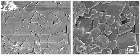
Figs. Comparison of secondary electron images of an aluminum-based ceramic specimen with charging (left) and without charging (right), taken at an accelerating voltage of 10 kV.
Left image (with charging) shows an anomalously bright area at the upper left. Bright and dark lines are seen from left to right (scan direction of the electron probe). Furthermore, the topographic contrast is weak in the whole image.
Right image (without charging) exhibits the removal of charging owing to the application of gold-palladium coating. Anomalous contrast is not seen unlike the left image, and a clear topographic contrast is seen.
関連用語から探す
説明に「帯電現象」が含まれている用語


