電界放出電子銃
電界放出電子銃
field-emission electron gun, FE electron gun, FEG
[目次:装置]
電界放出現象を利用した電子銃。
電界放出現象とは、固体の表面に強い電界をかけたとき、電子を固体内に閉じ込めていたポテンシャル障壁が低くなると同時に薄くなり、電子がトンネル効果によって真空中に放出される現象のこと。
陰極(エミッター)には、先端の曲率半径が100nm程度のタングステン(W)〈310〉単結晶が用いられる。10-8 Paの超高真空の環境で、エミッター先端周辺に強電界を作り、電子を放出させる。エミッターは室温で使うため、冷陰極エミッターと呼ばれる。光源(仮想光源)の大きさは5~10 nmと小さく、輝度が熱電子放出電子銃に比べて3桁も高い(108 A/cm2sr)ために、高分解能SEM用の電子銃として用いられる。放出電子のエネルギー幅(約0.3eV)が、熱電子放出電子銃より1桁、ショットキー放出電子銃の半分程度と小さいため、対物レンズの色収差の影響が大きくなる低加速電圧でも高分解能が得やすい。寿命は数年である。
ただし、電界放出電子銃は室温で動作するため、超高真空であってもエミッターへの残留ガスの吸着や、放出電子によってイオン化された残留ガス分子がエミッターを衝撃することが避けられず、放出電流が不安定になりやすい。これを防ぐために、フラッシングというエミッターの瞬間的な加熱を行い、エミッター表面の清浄化を行う必要がある。エミッターからの電子の放出角が、熱電子放出電子銃やショットキー電子銃に比べて大きいため、集束レンズの収差の影響を受けやすく、プローブ電流は大きくできない。
したがって、高分解能に有利な電子銃ではあるが、安定で大きなプローブ電流が長時間必要な、波長分散形X線分光器(WDS)による元素分析や、EBSDによる結晶解析などを主目的とする使い方には不向きである。
図は、電界放出電子銃の基本的な構造を示す。引き出し電極に印加された引き出し電圧によって所定の電流量の電子をエミッター先端から放出させる。さらに加速電極に印加された加速電圧によって所定のエネルギーに加速される。
電界放出電子銃の基本構造⇒図
An electron gun that utilizes the field emission phenomenon.
The field emission phenomenon means as follows: When a strong electric field is applied to the surface of a solid, the potential barrier which encloses the electrons in the solid becomes low and thin, and the electrons are released into vacuum by the tunneling effect.
A <310> single crystal of tungsten (W), with a radius of a curvature of its tip being about 100 nm, is used as the cathode (emitter) of the field-emission electron gun (FEG). The strong electric field is generated around the emitter tip for the electrons in the solid to emit from the solid surface. The gun is operated in an ultra-high vacuum of 10-8 Pa to avoid contamination of the tip due to residual gases. Since the emitter is operated at room temperature, this is called a cold-cathode emitter.
The diameter of the virtual source is as small as 5 to 10 nm. The brightness of FEG is about 108 A/cm2sr., which is about three orders of magnitudes higher than that of the thermionic-emission gun. Thus, FEG is used for a high-resolution SEM. FEG has a lifetime of several years.
Another feature of FEG is a very small energy spread (about 0.3 eV) of the electrons emitted from the cathode. This energy spread is about one order of magnitude smaller than that of the thermionic-emission gun, and about one-half smaller than that of the Schottky-emission electron gun. Thus, FEG helps to acquire a high-resolution image at a low accelerating voltage where the chromatic-aberration effect of the objective lens becomes serious.
However, since FEG is operated at room temperature, the emission current is likely to fluctuate even in an ultra-high vacuum because the emitter surface is contaminated by adsorption of residual gases, and is bombarded by gas molecules ionized by the emitted electrons. To prevent the contamination of the emitter surface, "flashing" is needed to rapidly heat the emitter for cleaning the emitter surface. Since the emission angle of the electrons from the emitter is larger than the thermionic-emission gun and the Schottky-emission electron gun, the electron probe is likely to suffer the aberration of the condenser lens, thus largely decreasing the probe current.
Therefore, FEG is advantageous for high-resolution imaging but disadvantageous for elemental analysis using a wave-length dispersive X-ray spectrometer (WDS) and for crystal orientation analysis by electron backscatter diffraction (EBSD), both of which require a stable and high probe current over a long time.
Figure shows the basic structure of FEG. The emission current is controlled by the voltage applied to the extraction anode. The emitted electrons are accelerated up to a desired energy by the voltage applied to the acceleration anode.
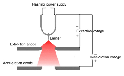
Fig. Basic structure of FEG.
関連用語から探す
説明に「電界放出電子銃」が含まれている用語


