電子プローブ径
電子プローブ径
electron-probe diameter, probe diameter
[目次:装置]
試料表面にフォーカスされた電子プローブの直径を電子プローブ径(プローブ径)という。プローブ径dの定義は様々であるが、次式が広く用いられている。※1
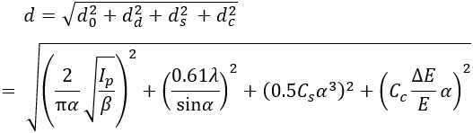
上段の式は、収差がない場合の光源によるプローブ径d0、回折収差によって決まるプローブ径dd、球面収差によって決まる最小錯乱円のプローブ径ds、色収差によって決まる最小錯乱円のプローブ径dcのそれぞれの二乗平均平方根が試料表面上のプローブ径dとなることを示す。
下段の式は、d0、dd、ds、dcを具体的に記述したもので、Ipはプローブ電流、βは電子銃の輝度、αは電子プローブの集束半角、λは電子の波長、Csは対物レンズの球面収差係数、Ccは対物レンズの色収差係数、Eは電子線のエネルギー、ΔEは電子線のエネルギー幅である。上記の式から、プローブ径dは、電子プローブの集束半角αの関数であることが分かる。
図1は、タングステンフィラメントの熱電子銃を搭載した汎用型SEMで、加速電圧20 kV における電子プローブ径dを集束半角αの関数としてプロットした結果である。ここで用いた各パラメータは以下の通りである※2 E=20 keV、ΔE=1 eV、Cs=50 mm、Cc=20 mm、β=7×10⁴ A/cm2/sr、Ip=1 pA、10 pA、100 pAの3通り。プローブ電流を3通り選んだのは、小さなプローブ電流で高分解能観察を目的とした使い方をする場合と、大きなプローブ電流で分析を目的とした使い方、および両者の中間的な使い方を想定したためである。
このグラフから、熱電子銃を搭載した汎用型SEMの加速電圧20 kV (E=20 keV) においては、Ipが100 pAでは、dを決める主要因が光源のプローブ径d0と球面収差による広がりdsであることが分かる。プローブ電流Ipが1 pA の場合は、色収差による広がりdcの影響も加わる。それぞれの場合のプローブ径dの最小値は~33 nmおよび~7 nmである。プローブ径dを小さくして空間分解能の高い画像を取得するためには、dを最小にするαを数値計算により求め、対物レンズ絞りの径を選択するか、もしくはαを制御するレンズの励磁によって、そのαの値に設定する。
図2は、ショットキー型電子銃を搭載したSEMで、加速電圧が1 kVと20 kVの場合の、電子プローブ径dの集束半角αに対する変化をプロットした結果である。用いたパラメータは、以下の通りである※2
E=1 keVと20 keVの2通り、ΔE=0.5 eV、Cs=4 mm、Cc=2 mm、β=1×10⁸ A/cm2/sr、Ip=1 pA 。
このグラフから、ショットキー型電子銃を搭載したSEMの電子プローブ径dの最小値を決める主要因は、加速電圧 20 kVの場合、回折収差による広がりddと球面収差による広がりdsであり、加速電圧1 kV では球面収差による広がりdsと色収差による広がりdcであることが分かる。それぞれの場合のプローブ径dの最小値は~1 nmおよび~7 nmである。加速電圧を下げると、色収差の効果によってプローブ径は大きくなる。 タングステンフィラメントの熱電子銃を搭載した汎用型SEMでは、最小プローブ径~7 nm は高い加速電圧 20 kV で達成できたが、ショットキー型電子銃を搭載したSEMでは低加速電圧1 kV で得られることが分かる。これは、ショットキー型電子銃のプローブ径d0がタングステンフィラメントの熱電子銃の場合に比べて小さいからである。
※1 L. Reimer, Scanning Electron Microscopy, Springer, Berlin, Germany, p. 30-34 (1998).
※2 L. Reimer, Scanning Electron Microscopy, Springer, Berlin, Germany, p. 32 (1998).
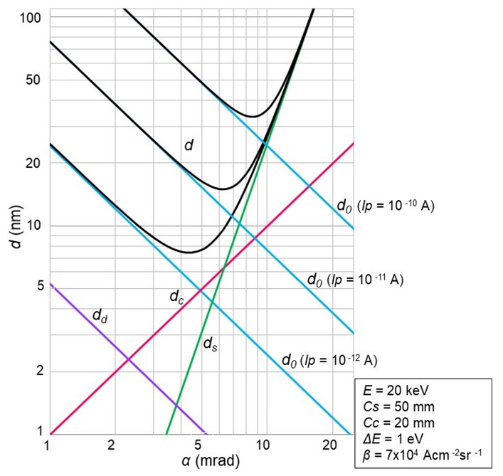
図1 熱電子銃を装着した汎用型SEMのプローブ径d (黒線)。
横軸は電子線の集束半角α 。
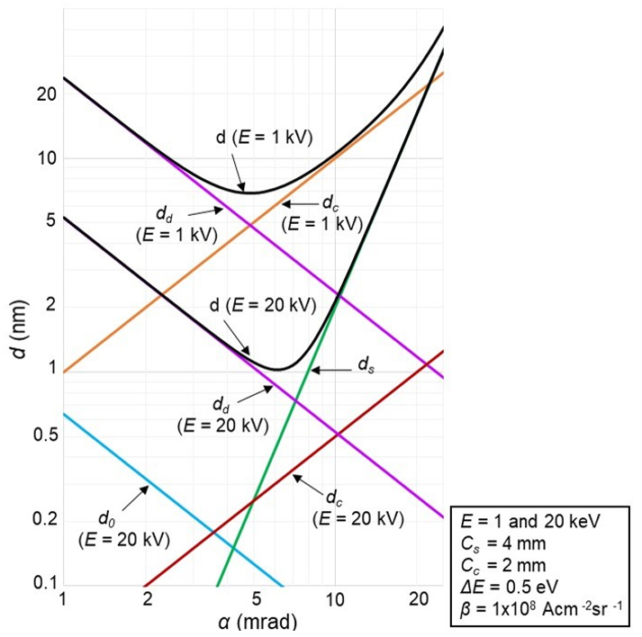
図2 ショットキー型電子銃を搭載した高分解能SEMのプローブ径d (黒線)。
横軸は電子線の集束半角α 。
The electron-probe diameter (probe diameter) means the diameter of the incident electron probe focused onto the specimen surface.
The following equation is widely used for the definition of the probe diameter.
The upper equation represents that the probe diameter d at the specimen surface is obtained by the root mean square of four terms, or d0 (probe diameter obtained by an electron source with no aberration), dd (probe diameter determined by diffraction aberration), ds (probe diameter of the minimum confusion circle determined by spherical aberration) and dc (probe diameter of the minimum confusion circle determined by chromatic aberration). The lower equation expresses specific descriptions of d0, dd, ds and dc. Here, Ip is the probe current, β is the brightness of the electron gun, α is the convergence semi-angle of the electron probe, λ is the electron wavelength, Cs is the spherical aberration coefficient of the objective lens, Cc is the chromatic aberration coefficient of the objective lens, E is the energy of the electron beam and ΔE is the energy spread of the electron beam. The equation shows that the probe diameter d is a function of the convergence semi-angle α of the electron probe.
Fig. 1 shows the probe diameter d as a function of the convergence semi-angle α for an ordinary SEM equipped with a thermionic-emission electron gun (tungsten filament) operating at an accelerating voltage of 20 kV. The parameters used here are as follows: E=20 keV, ΔE=1 eV, Cs=50 mm, Cc=20 mm, β=7×10⁴ A/cm2/sr, and Ip=1 pA, 10 pA and 100 pA (three cases). It is noted that the three probe currents Ip correspond to the cases: a small probe current for high spatial-resolution observation, a large probe current for element analysis, a medium probe current for compromising high-resolution observation and element analysis.
The black curve for Ip = 100 pA shows that the probe diameter d is determined mainly by d0 and ds, where d0 is the probe diameter due to the electron source and ds is the probe diameter due to spherical aberration. The black curve for Ip = 1 pA indicates that the probe diameter d suffers the contribution of the probe spread due to chromatic aberration dc. It is seen that the smallest probe diameter d is ~33 nm for the former case (Ip : 100 pA) and ~7 nm for the latter case (Ip : 1 pA). In order to decrease the probe diameter d for acquiring a high spatial-resolution image, first α that minimizes d is examined by numerical calculations, and then α is set to the calculated value by selecting an objective aperture (diameter) or by adjusting the excitation of the lens to control α.
Fig. 2 shows the probe diameter d as a function of the convergence semi-angle α for an SEM equipped with a Schottky electron gun operating at accelerating voltages of 1 kV and 20 kV. The parameters used are as follows: E=1 keV and 20 keV (two cases), ΔE=0.5 eV, Cs=4 mm, Cc=2 mm, β=1×10⁸ A/cm2/sr and Ip=1 pA . In the case of an SEM equipped with a Schottky electron gun, the probe diameter d is determined mainly by dd (probe spread due to diffraction aberration) and ds (probe spread due to spherical aberration) for the accelerating voltage of 20 kV, but is determined mainly by dd (probe spread due to diffraction aberration) and dc (probe spread due to chromatic aberration) for the accelerating voltage of 1 kV. It is seen that the smallest probe diameter d is ~1 nm for the accelerating voltage of 20 kV and ~7 nm for the accelerating voltage of 1 kV. As the accelerating voltage is lowered, the probe diameter becomes large due to the increase of the chromatic aberration.
In the case of an ordinary SEM equipped with a thermionic-emission electron gun, the smallest probe diameter of ~7 nm is obtained only at a high accelerating voltage of 20 kV. On the other hand, in the case of an SEM equipped with a Schottky electron gun, a similar diameter of ~7 nm is obtained even at a very low voltage of 1 kV. This is because d0 (probe diameter obtained by the electron source with no aberration) of the Schottky electron gun is significantly smaller than that of the thermionic-emission electron gun (tungsten filament).
Fig. 1 Probe diameter d (black line) for an ordinary SEM equipped with a thermionic-emission electron gun. The abscissa represents convergence semi-angle α.
Fig. 2 Probe diameter d (black line) for a high-resolution SEM equipped with a Schottky electron gun. The abscissa represents the convergence semi-angle α.
関連用語から探す
説明に「電子プローブ径」が含まれている用語


