二次電子
二次電子
secondary electron, SE
[目次:理論]
入射電子(一次電子)の試料内での非弾性散乱によって、試料を構成する原子から励起された電子で、そのエネルギーを50eV以下で定義することが多い。 入射電子による二次電子の励起は、試料の深さとは無関係に起こっているが、二次電子のエネルギーは小さく試料内で散乱されるため、試料の表面に到達できるのは、試料の浅い部分で励起されたものだけである。二次電子が試料表面から飛び出せる深さ(脱出深さ)は金属試料で5~10 nmである。したがって、電子線を試料表面に対して垂直ではなく斜めに入射すると飛び出してくる二次電子は多くなる。 下図(a)に、20 keVの一次電子が試料に入射したときに、試料の表面から放出される電子のエネルギースペクトルを示す。左側の大きなピークが二次電子によるものである。それ以上のエネルギーを持って放出される電子のほとんどは反射電子(後方散乱電子)で、幅広いエネルギー分布を持つ。反射電子の分布の中に見られる小さなピークはオージェ電子によるものである。 試料から放出される二次電子の多くは、入射電子によって照射点近くで直接励起されたもので、SE1と呼ばれる。SE1は入射点近傍の試料の形状(入射点の試料の傾き)や物質の違い(仕事関数)の情報を持っており、二次電子像の形成に用いられる。
ただし、二次電子には、SE1とは異なる発生要因のものもある。入射電子のエネルギーが大きくなる(加速電圧が高くなる)と、入射電子の拡散領域が大きくなり、入射点から離れた部位に反射された電子によっても二次電子が励起される。この二次電子は、SE2と呼ばれる。また、試料から飛び出した反射電子が対物レンズや検出器などの構造物に当たって二次電子を励起することもある。これはSE3と呼ばれる。SE2とSE3は、二次電子像のバックグラウンドを形成し像のコントラストを下げるSE1、SE2、SE3の発生を図(b)に示す。
図(a) 一次電子の入射によって試料から放出される電子のエネルギースペクトル (一次電子のエネルギーが20 keVの場合) ⇒図
図(b) SE1、SE2、SE3放出の違い ⇒図
“Secondary electron(s)” mean the excited electrons having an energy being defined to be less than 50 eV among all of the excited electrons, which are generated from the constituent atoms of a specimen by inelastic scattering of the incident electrons (primary electrons) in a specimen.
Although the secondary electrons are excited irrespective of the depth of the specimen, the electrons which can reach the specimen surface are limited only to those excited near the surface of the specimen because the secondary electrons have small energies and are scattered in the specimen. That is, the escape depth of secondary electrons from the specimen is as small as 5 to 10 nm for most metals. Thus, the secondary electrons are emitted more at an oblique incidence of the incident probe onto the specimen surface than at a perpendicular incidence of the probe.
Fig. (a) shows an energy spectrum of the emitted electrons from a specimen surface for a primary electron beam of 20 keV. A large peak at the left is due to the secondary electrons, extending to about 50 eV. The electrons with more than 50 eV are backscattered electrons (reflected electrons) existing over a wide energy range. Small peaks seen in the range of backscattered electrons are attributed to the Auger electrons.
The major part of secondary electrons is excited directly by the incident electrons along the incident electron path and emitted only near the specimen surface. These secondary electrons are called “SE1(s).” SE1 is used to form a secondary electron image, which possesses information on the specimen shape (angle of the specimen surface against the incident electron beam) at the incident electron position and on the work function of the specimen.
It should be noted that there is another type of secondary electrons. When the incident electron energy is large (accelerating voltage being high), the diffusion region of the incident electrons becomes large. The backscattered electrons (reflected electrons) into a region distant from the incident electron path excite secondary electrons. These secondary electrons are called “SE2(s)”, which form the background of the secondary electron image (formed by SE1), degrading the image contrast. In addition, if the incident electron energy is as large as a few 10 eV, the backscattered electrons coming out from the specimen hit the SEM components (objective lens, detector, etc.) and can excite secondary electrons from the components. Those secondary electrons are called “SE3(s)” and form the background of the secondary electron image or decrease the contrast of the secondary electron image. The generation process of SE1, SE2 and SE3 is shown in Fig. (b).
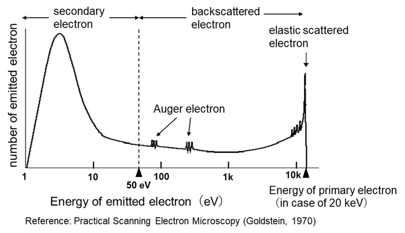
Fig.(a) Energy spectrum of electrons emitted from a specimen at a primary electron probe of 20 keV.
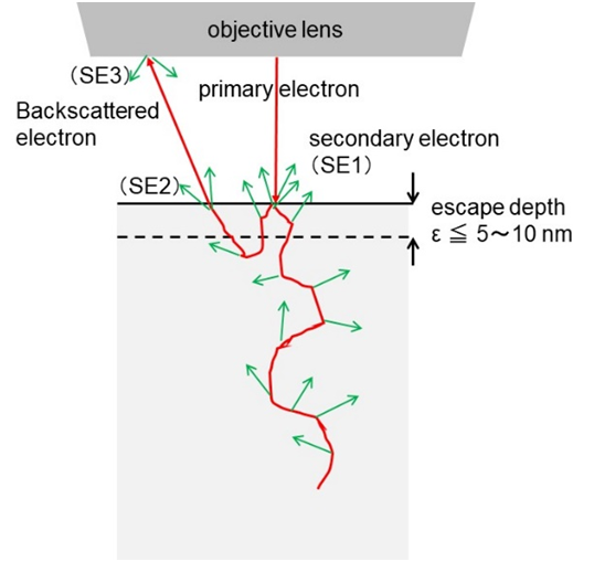
Fig.(b) Generation processes of SE1, SE2 and SE3.
関連用語から探す
説明に「二次電子」が含まれている用語


