反射電子
反射電子
reflected electron, backscattered electron, RE, BSE, BE
[目次:理論]
入射電子(一次電子)が試料に照射された際に、散乱の過程で後方散乱したもの。このため、後方散乱電子とも呼ばれる。図(a)は、20 keVの入射電子による放出電子のエネルギースペクトルである。反射電子は、約50 eVから最高値の20 keVまでの広い幅を持つ。スペクトルの中央付近に見られる小さなピークはオージェ電子である。
反射電子が広いエネルギー幅を持つ理由は、入射電子(一次電子)が入射点近傍で弾性散乱してエネルギーを失わないまま試料外に飛び出すばかりでなく、非弾性散乱を繰り返してエネルギーを失いつつ後方散乱されるものがあるからである。
反射電子は二次電子に比べてエネルギーが高いため、その脱出深さは二次電子の場合に比べて約2桁大きい。具体的には、入射電子のエネルギーが15 keVの場合、アルミニウムと鉄に対する反射電子の脱出深さは、それぞれ約0.7μmと約0.2μmである。試料の深い部位から放出した反射電子は、分解能の低下を招く。
反射電子放出率の原子番号依存性を図(b)に示す。反射電子放出率は原子番号の増加に伴って単調に増加することがわかる。反射電子像では、この特性を利用して、試料中の組成の違いを明らかにできる。なお、二次電子放出率は原子番号との間に特定の相関がないので、二次電子像では組成の違いを明らかにすることはできない。
反射電子放出量が、試料表面の入射電子に対する角度の違いによって変化することを図(c)に示す。反射電子の放出量は入射電子が鏡面反射する方向で大きくなる。したがって、検出器をある位置に固定すると、試料の凹凸によるコントラストが得られる。反射電子の強度は試料の凹凸に非常に敏感に変化するので、エッジを持たないなだらかな起伏に対してもコントラストがつく。一方、二次電子像で見られるエッジ効果がないため、微細で急峻なエッジを持つ凹凸に対しては二次電子像のようなシャープさは得られない。
なお、反射電子は、試料表面近傍で二次電を励起したり、試料から飛び出したあとで対物レンズなどのSEMの構造物に衝突して、二次電子を励起したりすることがあり、それらの二次電子は、二次電子像の像質を低下させる。
(一次電子のエネルギーが20 keVの場合)。
約50 eVから最高値の20 keVまでのエネルギーを持って放出される電子を反射電子という。スペクトルの中央付近に見られる小さなピークはオージェ電子である。
反射電子放出率は原子番号の増加に伴って単調に増加する。
反射電子の放出量は入射電子が鏡面反射する方向で大きくなる。検出器をある位置に固定すると、検出器方向に直進したものだけが検出され、それ以外の方向に放出されたものは検出されないため、あたかも検出器から試料表面を照明しているような像が得られる。このことを利用して試料の凹凸によるコントラストが得られる。
"Backscattered electron(s)" mean the electrons which are scattered backward against the incident electrons (primary electrons) in the electron-scattering process. These electrons are sometimes called "reflected electrons". Fig. (a) shows an energy spectrum of electrons emitted from a specimen for an incident electron probe of 20 keV. The energy of the backscattered electron ranges from about 50 eV up to 20 keV. Small peaks around the center of the spectrum are attributed to Auger electrons.
A wide energy spread of the backscattered electron is due to the fact that the incident electrons repeat not only elastic scattering but also inelastic scattering along the incident electron path, and the electrons suffered by energy loss are emitted from the specimen.
Since the energy of the backscattered electron is much larger than that of the secondary electron, the escape depth of backscattered electrons from the specimen is about two orders of magnitudes larger than that of secondary electron. As an example, when the incident electron energy is 15 keV, the escape depth of backscattered electrons for Al and Fe is about 0.7 μm and 0.2 μm, respectively. The backscattered electrons emitted from the deep region degrade the resolution.
Fig. (b) shows the dependence of the backscattered electron coefficient on the atomic number. As the atomic number increases, the backscattered electron coefficient increases. Owing to this characteristic feature, the backscattered electron image reveals the compositional difference in the specimen. It should be noted that, since the secondary electron emission coefficient has no relation with the atomic number, the secondary electron image cannot distinguish the compositional difference.
Fig. (c) shows the change of the backscattered electron emission with the angle of the specimen surface against the incident electron probe. The backscattered electron emission is large in the direction of the specular reflection of the incident electrons with respect to the specimen surface. Thus, when the detector is fixed at a certain position, the topographic image of the specimen is obtained. Since the backscattered electron intensity is very sensitive to the topography of the specimen, the image can reveal even gentle undulations of the specimen without sharp edges. It is, however, noted that the backscattered electron image does not provide the edge effect which appears in the secondary electron image. Thus, the backscattered electron image is less sharp than the secondary electron image for a specimen with very fine and sharp edges.
It is noted that backscattered electrons can excite secondary electrons (SE2) near the specimen surface, and also hit the SEM components (objective lens, etc.) and excite secondary electrons (SE3). Those electrons degrade the quality of the secondary electron image.
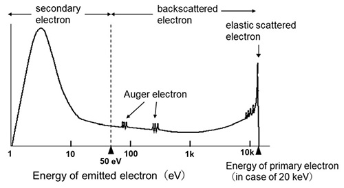
Fig.(a) Energy spectrum of electrons emitted from a specimen for a primary electron probe of 20 keV.
Backscattered electrons are the electrons emitted from the specimen with an energy ranging from about 50 eV up to 20 keV. Small peaks around the center of the spectrum are attributed to Auger electrons.
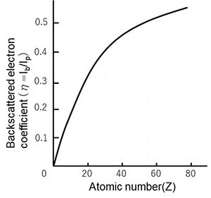
Fig.(b) Dependence of backscattered electron coefficient on the atomic number.
As the atomic number increases, the backscattered electron coefficient also increases.
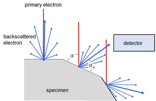
Fig.(c) Dependence of backscattered electron emission on the angles of the specimen surface against the incident electron probe.
The backscattered electron emission is large in the direction of specular reflection of the incident electron probe with respect to the specimen surface. When the detector is fixed at a certain position, the detector detects only the backscattered electrons traveling straight into the detector and thus, an image as if the specimen illuminated from the detector is obtained. Owing to this characteristic feature, the topographic image of the specimen is obtained.
関連用語から探す
説明に「反射電子」が含まれている用語


