反射電子組成像
反射電子組成像
compositional image in BE mode, compositional image in BSE mode, BSE compositional image
[目次:理論]
試料の平均原子番号の差(組成の違い)を示す反射電子像。
試料の組成分布や単一組成領域の大きさを知ることができる。
エネルギー分散型X線分光器(EDS)や波長分散型X線分光器(WDS)による元素分析を行うための事前観察にも使われる。
反射電子の検出には、対物レンズと試料の間に、入射電子に対して対称に置かれた環状の半導体素子が用いられ、その素子を2分割もしくは4分割した物もある。2分割した検出器を使用した場合、反射電子組成像は、二つの検出器の出力信号の和を取ることによって得られる。
また、2分割した検出器の出力信号の差を取ると、組成の違いによるコントラストが打ち消され、試料の凹凸による像が得られる。
図にダイヤモンド砥石の反射電子組成像と反射電子凹凸像を示す。
左の組成像ではダイヤモンドの粒子が黒く見えている。ダイヤモンドの反射電子放出率が小さいためである。白く見えている部分は反射電子放出率が大きい、すなわち炭素より重い原子が存在する場所である。二つの検出器からの出力信号の和を取っているために、試料の凹凸の効果は打ち消されている。
右の凹凸像では、二つの検出器からの出力信号の差を取っているために、組成の違いによるコントラストは消え、表面の凹凸のみが見えている。
加速電圧: 10 kV, 試料: ダイヤモンド砥石
左図の組成像では、反射電子放出率の小さいダイヤモンド粒子が黒く見えている。右図の凹凸像では、組成によるコントラストは消え、試料の凹凸のみが見えている。
"BSE compositional image" means a backscattered electron image which exhibits the difference in the average atomic number (compositional difference) in a specimen.
This image reveals the compositional distribution and the size of a mono-compositional area. In addition, the BSE compositional image is effectively used to specimen observation in advance of elemental analysis using an energy dispersive X-ray spectrometer (EDS) or a wavelength dispersive X-ray spectrometer (WDS) because the image provides an overall composition of the specimen.
For detecting backscattered electrons, an annular semiconductor device (detector) placed symmetrically against the incident (primary) electron beam is used. The detector which is divided into a pair of two segments or a pair of four segments is also available.
When the two-segmented detector is used, the BSE compositional image is obtained by adding the output signals from both pair of segments.
To the contrary, when subtracting the output signals between each pair of segments by the use of this detector, the contrast due to compositional difference is canceled out and instead, the image formed by specimen topography is obtained.
Figures below show a BSE compositional image (left) and a BSE topographic image (right) of a diamond grindstone.
In the left compositional image, diamond particles appear dark (black) because the backscattered electron emission coefficient is small for diamond. To the contrary, the regions where atoms heavier than carbon exist, are seen to be bright (white). Since the sum of the addition of two output signals from the two detectors is collected, the topographic effect in the specimen is canceled out.
In the right topographic image, the difference of the output signals between the two detectors is collected, and thus the compositional contrast disappears and only the topographic contrast of the specimen is observed.
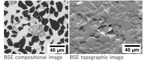
Fig. Comparison of BSE compositional image and BSE topographic image of a diamond grindstone, taken at an accelerating voltage of 10 kV
In the left compositional image, diamond particles are seen to be dark (black) because of a small backscattered electron emission coefficient of diamond. In the right topographic image, the compositional contrast disappears and only the topography of the specimen is observed.
関連用語から探す
説明に「反射電子組成像」が含まれている用語


