レビューSEM
レビューSEM
Review SEM
[目次:装置]
数千ステップ(作業の最小単位)におよぶ半導体の製造工程で発生するウエハ表面の異物やキズ、パターン欠けなどの欠陥を検出・分類・マッピングするための検査装置で、ウエハ上のチップ(ウエハ上に細かく仕切られた領域のこと)製造における歩留りやチップの信頼性の向上に寄与する。検出する異物や欠陥のサイズは概ねそのチップを製造したプロセスの最小加工線幅の半分程度とされている。
当初はウエハ表面での光の散乱の違いを検出して異物や欠陥を見つけていたが、デバイスの微細化により最小加工寸法が500 nmとなった1990年頃から検査対象となる異物や欠陥も200 nm以下に微細化し、それ以降はレビュー(検査)装置が光学式からSEM式に切り替わった。2020年代以降の最小加工寸法は5~10 nmとなり、対象となる微小異物や欠陥を検出するためには2 nm以下の像分解能が必要になった。そのため高分解能観察に向いているセミインレンズ型対物レンズやリターディング機能(減速法の一種)を備えたSEMが使われている。
レビューSEMはスループット短縮のため、(1) 300 mmφウエハを全面検査する代わりにウエハ内の特定領域5~数十点を指定した検査や、(2)トランジスタのゲート加工やコンタクトホール形成、ファインピッチ配線層形成など,異物や欠陥の歩留りに及ぼす影響が大きい工程に限った検査をすることがある。
レビューSEMによる検査時にはウエハ上に既にトランジスタやキャパシタなどが形成されている場合が多く、トランジスタの素子特性に入射電子が影響を及ぼさないように、加速電圧は0.5~0.7 kV程度に抑えられている。また形状と組成の情報を集めるために二次電子や反射電子を効率良く収集できる鏡筒内検出器が用いられる。
図1に一般的なレビューSEMの模式図を示す。成膜やエッチング等の製造装置から自動搬送されてきたウエハをレビューSEMに挿入し(受け入れ)、測定の終わったウエハを取り出す(払い出し)ためのロードポートが装置前面に配置されている。検査はレシピ(業界標準で決められた特定の手順)に基づいて自動実行されるので通常オペレーターはいないが、装置のメンテナンスのための制御卓を備える。SEMの鏡筒は気流や騒音による振動を防ぐために鏡体カバー(enclosure)で覆われている。
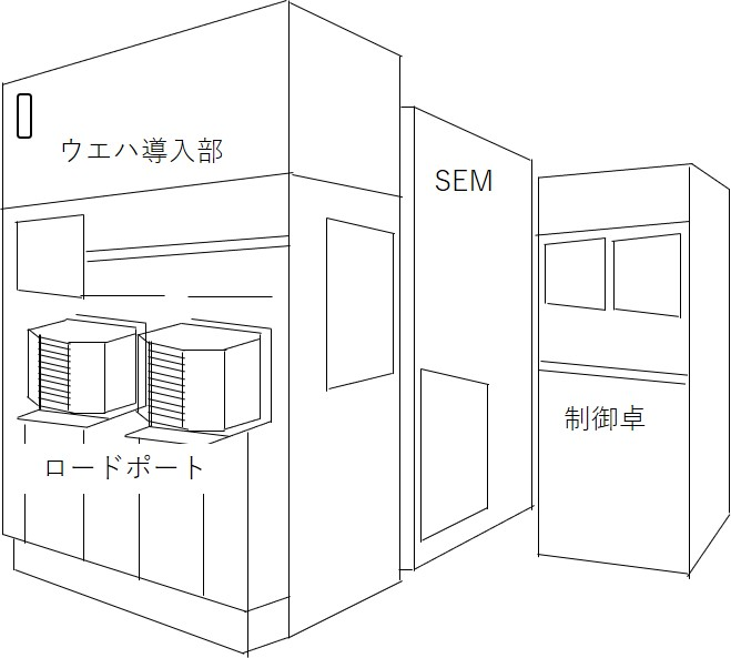
図.1 レビューSEM 外観模式図
レビューSEM装置には以下のような機能がある。
300mmφウエハを全面観察できる試料台を備える。
前工程内に設置されたウエハ搬送装置と接続され、検査ウエハの導入、検査、検査結果の出力、ウエハの次工程への払い出しが完全自動化されている。
検査結果は、業界標準であるSEMI Standardsに定められたフォーマットと通信方式を使用して、製造工程のデータを管理するサーバーに転送される。
ユーザーがあらかじめ設定した基準以上の数の欠陥があったウエハは次工程に搬送せず待機させる。
欠陥の位置座標の記録とマッピング、形状と組成による欠陥の分類し、マッピングによる複数枚のウエハ間の異物分布を比較することができる。
回路パターンが形成されたウエハ表面の検査では、隣接するチップの同じ場所を観察した結果との差を検出することによって欠陥を出力する。
帯電による像質変化(電位コントラスト)を利用してコンタクトホール(上下の配線層とトランジスタを接続する金属材料を埋め込んだ竪穴)の高抵抗部位を検出する欠陥検査機能を備える。
他の検査装置と同様、検査中に発生する異物によって歩留りや信頼性に影響を受けないようになっている。
図2にレビューSEMによる異物検出の例を示す。この検査例には2種類の異物があり、金属などの重元素を多く含む異物が青、Siを主成分とする比較的軽元素からなる異物が赤の点で示されている。重元素は製造装置由来、軽元素は製造工程(プロセス反応)由来の異物であることが多い。
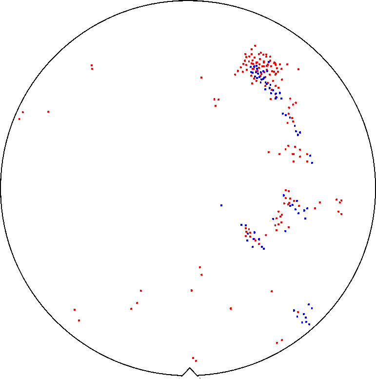
図.2 レビューSEMにより検出された異物のマッピング例
形状と組成により分類された二種類の異物の位置情報が表示されている。
Review SEM is an inspection system to detect, classify and map foreign materials and defects (scratches, pattern failures, etc.) on a semiconductor wafer surface, which occur in semiconductor manufacturing processes consisting of several thousands of steps (step means a smallest unit of process). The Review SEM serves to improve the yield of fabrication of chips (finely divided area on the wafer) and reliability of the fabricated chips. The size of the foreign materials and defects to be detected by the Review SEM, is approximately half the minimum line width of the chip manufacturing process.
In the early stages, the foreign materials and defects were identified by detecting differences in light scattering on the wafer surface. However, from around 1990 the minimum processing dimension reached down to 500 nm due to device miniaturization, and the foreign materials and defects to be inspected became smaller than 200 nm. Since then, the inspection system was replaced from the optical to SEM system. Furthermore, entering into 2020s, the minimum processing dimension became 5 to 10 nm, and a high image resolution of 2 nm or better was required for detecting very-small foreign materials and defects of interest. For this reason, SEMs equipped with a semi-in-lens objective lens and a retarding function (a type of deceleration methods), which are suited to high-resolution observation, are currently used.
In order to shorten the throughput of the inspections, the Review SEM can be used for (1) inspections specifying five to several tens of areas on the wafer instead of inspecting the entire surface of a 300 mm diameter wafer, and (2) inspections of the limited processes, where the foreign materials and defects give significant effects on the yield of the chips, such as transistor gate processing, contact hole etching and fine-pitch wiring layer patterning.
In many cases, transistors and capacitors are already fabricated on the wafer at the time of inspection by the Review SEM. Thus, the acceleration voltage is kept at around 0.5-0.7 kV to prevent incident electrons from affecting the device characteristics of the transistor. In order to collect information on shape and composition, an in-column detector is used, which can efficiently collect secondary and backscattered electrons.
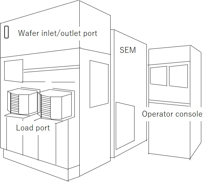
Fig. 1 illustrates a schematic of a typical Review SEM instrument. The load port is placed at the front of the instrument to insert wafers automatically transported from the manufacturing equipment for deposition and etching into the Review SEM (input), and to remove wafers from the instrument after finishing the measurement (output). Wafer inspection is carried out automatically according to the recipe (specific procedure defined by the industry standard), thus, usually there is no operators but an operator console is provided for maintenance of the instrument. The SEM column is covered by an enclosure to protect the column from vibrations due to air flow and noise.
Fig. 1. Schematic of the external view of a Review SEM system.
The Review SEM system has following features.
The system is equipped with a specimen stage enabling observation of the entire surface of a 300 mm diameter wafer.
The system is connected to a wafer transfer system placed in the front-end process unit. The introduction of the inspected wafer, inspection, output of inspection results and transfer (output) of the wafers to the next process are fully automated.
Inspection results are transferred to a server which manages the data of manufacturing processes, using the format and communication system specified by “SEMI Standards”, the industry standard.
Wafers having a higher number of defects than the user’s pre-defined criteria are not transferred to the next process, but are subjected to standby.
The system can record and map the positional coordinates of defects, classify the defects by shape and composition, and compare the distribution of foreign materials between the other wafers by mapping.
When inspecting the wafer chip surfaces on which circuit patterns are formed, defects are displayed by detecting the difference between the results of observation of the same area of the adjacent chip.
The system is equipped with an inspection function that detects high resistance areas in contact holes (vertical holes filled with a metallic material that connect the upper and lower wiring layers and transistors) using changes in image quality due to charging (voltage contrast).
The Review SEM is made so that yield and reliability are not affected by foreign materials and defects generated during inspection, as with the other inspection systems.
Fig. 2 shows an example of detection of foreign materials using a Review SEM. There are two types of foreign materials in this example. Foreign materials containing many heavy elements (e.g. metals) are displayed by blue dots, and foreign materials consisting of relatively light elements (mainly Si) are displayed by red dots. Heavy elements often originate from a semiconductor manufacturing equipment and light elements from the manufacturing processes (process reactions).
Fig. 2. Example of mapping foreign materials detected using a Review SEM.
Positional information of the detected foreign materials, classified by shape, and composition, is displayed as a map.
関連用語から探す
説明に「レビューSEM」が含まれている用語


