カソードルミネッセンス
カソードルミネッセンス
cathodoluminescence
[目次:分光分析(EELS/EDS/電子構造)]
電子ビームの照射によって固体内の電子を励起して、その電子が空孔と再結合するときの発光(紫外光から赤外光)のことをカソードルミネッセンス(CL)と呼び、この励起と再結合の現象を用いて固体の電子状態を電子顕微鏡を用いて分析することができる。固体中の不純物や格子欠陥等によって価電子帯と伝導帯の間(禁制帯内)にできる各種の電子状態(エネルギー準位)を調べることから、無機材料の結晶構造の欠陥などを1μm以下の高い空間分解能でSEM像やSTEM/TEM像から得られる構造的情報と合わせて材料評価を行うことができる。また、特定タンパクの検出など、生物試料への応用も研究されている。
- 半導体の場合、入射電子によって価電子帯の電子が伝導帯に励起され、価電子帯には正孔が生成される(対生成という)。励起された自由電子と正孔はクーロン力によって結びつけられた対(自由励起子;低温で顕著に起こる)を形成する。自由励起子は不安定で任意の場所で再結合して発光する。また、生成された自由励起子を形成できない温度(通常室温以上)では電子および正孔は電荷のキャリアとして個別に半導体中を拡散する。キャリアがドナーやアクセプターとなる不純物原子に捕獲されると発光性の再結合が起こる。転位などの格子欠陥に捕獲されると非発光性の再結合が起こる。このことを利用すると、特定の波長を使ったCL像から不純物原子の空間分布が検出できる。 なお、試料の温度が上昇すると格子振動が大きくなり、格子振動を介した非発光性の再結合が増加し発光は弱まるので、多くの場合液体窒素温度程度またはそれ以下の低温で測定する必要がある。また、照射電子ビームの加速電圧が閾電圧(~100kV)を越えると点欠陥の生成が増加し、禁制帯内に深い欠陥準位が作られ、その準位を介した非発光性再結合が生じてCLの発光強度が減少するので、100kV以下の加速電圧で測定する必要がある。
- 絶縁体の場合、酸化物や硫化物中に添加した遷移金属元素のd電子や希土類元素のf電子がつくる不純物中心や、アルカリハライド結晶中の空孔に局在した電子(この状態を色中心という)などが禁制帯内に基底準位と励起準位を形成し、それらの準位間の電子遷移で発光が起こる。この発光位置から添加元素の位置情報が得られる。加速電圧の制限は特に厳しくない。
- 有機物では有機分子の最低非占有分子軌道(LUMO)から最高占有分子軌道(HOMO)への電子遷移によって発光する。局所的な情報は得られないが、有機分子の劣化や経年変化の情報が得られる。試料が電子線に弱いので低加速電圧での観察が求められる。
(東工大 山本直紀博士 執筆)
図1 カソードルミネッセンス(CL)検出システムの概念図 ⇒図1
電子ビーム入射により試料から放出された光は放物面ミラーによって集光され、反射されて平行光となり、電子顕微鏡の鏡筒外に導かれる。この光は、レンズ1(L1)を通り、レンズ2(L2)によってCCD検出器の前の分光器のスリット上に焦点を結ぶ。スリットを通った光の分光スペクトルはCCDにより記録される。パソコンからの信号によって偏向コイルを駆動して電子ビームを二次元的に走査し、各ビーム位置からの発光スペクトルをCCDにより逐次測定する。測定後に波長を選んで単色CL二次元像を表示する。試料のSTEM像またはSEM像とCL二次元像を照合することから、試料中の構造的欠陥と光学的性質との関係についての情報を得る。
発光は赤外光(波長1~2.5μm)から紫外光(波長200nm~380nm)に亘る。分光には紫外光、可視光、赤外光に対して、専用の回折格子および検出器が使われる。検出器の波長分解能は1nm(エネルギーにすると10meV以下)程度である。
図2 貫通する転位を含むGaN成長膜のTEM暗視野像、CL像とCLスペクトル(加速電圧80kV) ⇒図2
サファイア基板上にMOCVD法で成長させたGaN膜(膜厚 4μm)を基板側からイオンミリングにより薄膜化し、エッジの薄い領域で、試料を貫通する転位を含む領域を透過電子顕微鏡(TEM)とCLにより観察した結果を示す。
(a) TEM暗視野像。図中の矢印は転位を示す。
(b) 同じ領域を室温において波長366nm(3.39eV)の光を使って表示した単色CL像。試料の広い領域で自由励起子(FX)発光が起こっているのが見られる(明るい部分)。矢印で示した転位のところでは、キャリアが捕獲され非発光性再結合を起こすため、暗いコントラストを示している。
(c) 異なる試料温度で測定したCLスペクトル。主ピーク(P1)はGaNのFX発光、P2ピークは不純物が関与した発光、P3ピークはドナー・アクセプタ対発光(D,A)である。CL像で転位を明瞭に見るためにはバックグラウンドを形成するFX発光が重要である。 FX発光強度は温度の上昇とともに減少し、室温での強度は19Kに比べ2桁小さくなる。特に試料の薄い領域の観察など発光強度が弱い場合には低温での測定が必要である。転位の周囲のCL強度分布の解析からキャリアの拡散距離が求められる。
Electrons in a solid are excited by electron-beam irradiation leaving holes. The electrons recombine with the holes to emit light (ultraviolet to infrared). This phenomenon is called "Cathodoluminescence". Cathodoluminescence is utilized as a method to analyze the electronic structure of solids in an electron microscope. The method can measure local electronic states (energy levels) of impurities and defects, the electronic states being formed between the valence band and the conduction band (in the forbidden band). Thus, the method enables the evaluation of inorganic materials containing the structural defects with a high spatial resolution (better than 1 μm) by the combined use with structural information obtained from SEM / STEM / TEM images. Applications to biological specimens, such as detection of specific proteins, have also been studied.
- In the case of semiconductors, electrons in the valence band are excited to the conduction band by incident electrons with generating holes in the valence band (referred to as electron-hole pair generation). The excited electrons and holes form a pair (free exciton (FX): It occurs remarkably at low temperatures) bound by Coulomb force. Free excitons are unstable and recombine at arbitrary places and emit light. At room temperature or higher temperatures, the free excitons cannot be formed, thus the generated electrons and holes diffuse independently in the semiconductor as carriers. When they are trapped by impurity atoms creating donors and acceptors, radiative recombination occurs. When they are captured by lattice defects such as dislocations, non-radiative recombination occurs. For example, the distribution of impurity atoms can be detected from a CL image using a specific wavelength.
CL measurements of semiconductors have to be conducted at liquid nitrogen temperature or lower because the luminescence intensity weakens due to the increases of non-radiative recombination through the lattice vibrations. Also, the CL measurements have to be performed with an accelerating voltage less than 100 kV. : When the accelerating voltage of the incident electron beam exceeds the threshold voltage (approx. 100 kV), the generation of point defects increases. The point defects create deep defect levels within the forbidden band and non-radiative recombinations via those levels increase, causing decrease of the luminescence intensity. - In the case of insulators, impurity centers are formed by d-electrons of transition elements and f-electrons of rare earth elements when they are added in oxides or sulfides, and color centers are formed at vacancies in alkali halide crystals. These electrons trapped at such localized centers produce a ground level and an excited level within the forbidden band. Light emission occurs at the electronic transition between those levels, enabling positional information on additive elements to be obtained. Restriction on the accelerating voltage of the incident electron beam is not severe.
- In the case of organic materials, light is emitted by electronic transition from the lowest unoccupied molecular orbital (LUMO) of the organic molecule to the highest occupied molecular orbital (HOMO). Local information cannot be obtained, but information on degradation and aging of organic molecules can be obtained. Since the organic specimen is susceptible to electron-beam irradiation, observation at a low accelerating voltage is required.
(By Dr. Naoki Yamamoto, Tokyo Institute of Technology)
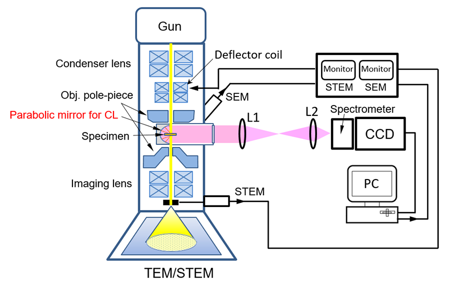
Fig.1 Schematic diagram of cathodoluminescence (CL) detection system.
Light emitted from a specimen in a STEM (SEM) by an incident electron beam is collected and reflected by a parabolic mirror, and becomes parallel light, then guided outside the electron microscope. This light passes through the lens 1 (L1) and is focused by the lens 2 (L2) onto the slit of the spectrometer in front of the CCD detector. The spectrum of the light passing through the slit is recorded with the CCD. The incident electron beam is two-dimensionally scanned using the beam deflector controlled with a computer, and the emission spectra from each beam position are successively acquired by the CCD. After measurement, a two-dimensional monochromatic CL image is displayed by selecting a specific wavelength. From the STEM or SEM image and the CL image of the specimen, the optical properties of the structural defects are obtained.
The luminescence ranges from infrared light (1 to 2.5 μm in wavelength) to ultraviolet light (200 nm to 380 nm). Specific gratings and detectors are used for ultraviolet-, visible- and infrared-light depending on the wavelength range. The wavelength resolution of the detector is approximately 1 nm (less than 10 meV in energy).
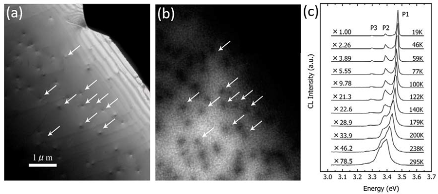
Fig.2 TEM dark field image, CL image and CL spectra of GaN epitaxial film containing the dislocations penetrating the specimen (accelerating voltage 80 kV)
A GaN epitaxial film grown by the MOCVD (metal organic chemical vapor deposition) method on a sapphire substrate (film thickness 4 μm) was thinned from the substrate side by ion milling. A transmission electron microscope (TEM) image and a CL image and CL spectra of a thin edge region containing the dislocations penetrating the specimen are shown.
(a) TEM dark field image. Arrows in the image indicate the dislocations.
(b) Monochromatic CL image of the same area in (a) taken at room temperature using an emission light with wavelength of 336 nm (3.39 eV).
It is seen that free exciton (FX) emission occurs in the whole area of the specimen (bright part). Dark contrast appears at the dislocations because the carriers are captured there and non-radiative recombination occurs.
(c) CL spectra measured at different specimen temperatures. The main peak (P1) is FX emission of GaN, the P2 peak is light emission associated with impurities, and the P3 peak is donor-acceptor pair emission (D, A). The FX emission intensity, which is important for elucidating the dislocation positions, decreases with increasing temperature, i.e., the intensity at room temperature is two orders of magnitude smaller than that at 19K. Thus, measurement at low temperature is necessary, especially for a thin specimen with a low emission intensity. From the analysis of the CL intensity distribution around a dislocation, the diffusion length of the carrier can be measured.
関連用語から探す
説明に「カソードルミネッセンス」が含まれている用語


