球面収差
球面収差
spherical aberration
[目次:レンズ系]
球面収差は円筒対称性を持つ3次の軸上幾何収差である。対物レンズの幾何収差の中で、高分解能観察の際に分解能の低下の最も大きな要因となっている。5次以上 (奇数次) の球面収差もあるが、電子顕微鏡では像への影響が大きい3次のみを扱う。
球面収差による電子線の広がり
球面収差があると、物面の光軸上の点から光軸と角度を持って射出した電子線はレンズを通過後、理想像面で光軸上に集まらず像面でない位置 (レンズ側) で光軸と交わる。そのため、物面の光軸上の点から射出した電子線は像面上に円状の広がった像を作る。広がりの量は球面収差係数 (Cs) と角度αの三乗の積、Csα3で与えられる(αは物体から射出する電子線が光軸となす角)。軸対称レンズではCsは常に正の値をとる。
TEMの場合
TEM観察では、対物レンズの中心付近に置かれた試料に対して電子線を平行に照射する。収差のない状態で結像できる角度範囲は、対物レンズにおける試料より後方の磁場の球面収差のために制限され、それより大きな角度の電子線は像面上で広がった像を作る (図(a))。球面収差の影響を受けない角度範囲は、アモルファス薄膜をシェルツァー・フォーカス条件で撮影した高倍率像のフーリエ変換図形のFirst Zeroの位置 (角度) として与えられる。図(b) の例では、加速電圧200 kVで、First Zeroの角度は13 mradであり、対応する像空間の空間分解能の数値は0.19 nmになる。
球面収差の測定
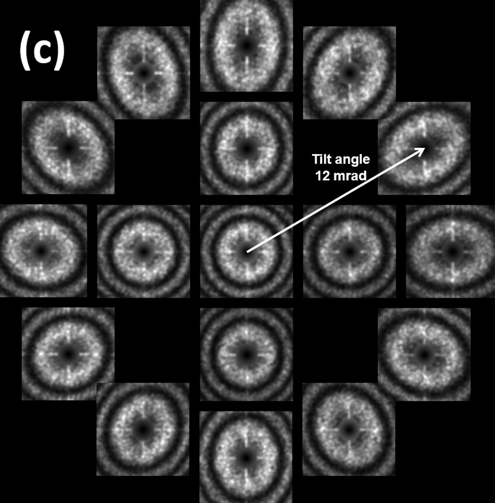
対物レンズの後方磁場に球面収差がある場合、光軸に対して電子線を傾斜させて試料に照射すると焦点ずれと二回非点収差が生じる。この焦点ずれと二回非点収差の値は、電子線の傾斜角を大きくすると増加する。これらの収差量の傾斜角依存性を測定することにより球面収差係数を求めることができる。実験的には、電子線の傾斜角と方位角を変えて撮影したDiffractogramの組である Diffractogram Tableau (図(c)) を用いて収差測定を行う。
STEMの場合
STEM観察では、対物レンズの中心付近に置かれた試料に対して電子線を集束させて照射する。対物レンズにおける試料より前方の磁場の球面収差のために、電子線が試料上で一点に集まる角度範囲が制限され、それより広角度の電子線は試料上に広がったプローブを作る (図(d)) 。球面収差が寄与しない角度領域は、電子波の干渉図形 (Ronchigram) 内の強度が一定の領域として与えられる。STEM像を取得するときは、収差のない角度範囲の電子線を集束レンズ絞りで選択し試料に照射する。図(e) の例では、加速電圧200kVで、球面収差が無い角度は11 mrad (図(e))、対応する実空間でのプローブサイズは0.14 nmである。
球面収差補正と5次球面収差
現在、(3次の) 球面収差の補正は可能になっており、6極子と転送レンズを使った収差補正器が主流になっている。3次の球面収差補正後、高角では5次の球面収差が補正の対象となる。5次の球面収差も上記の収差補正装置で補正できる。
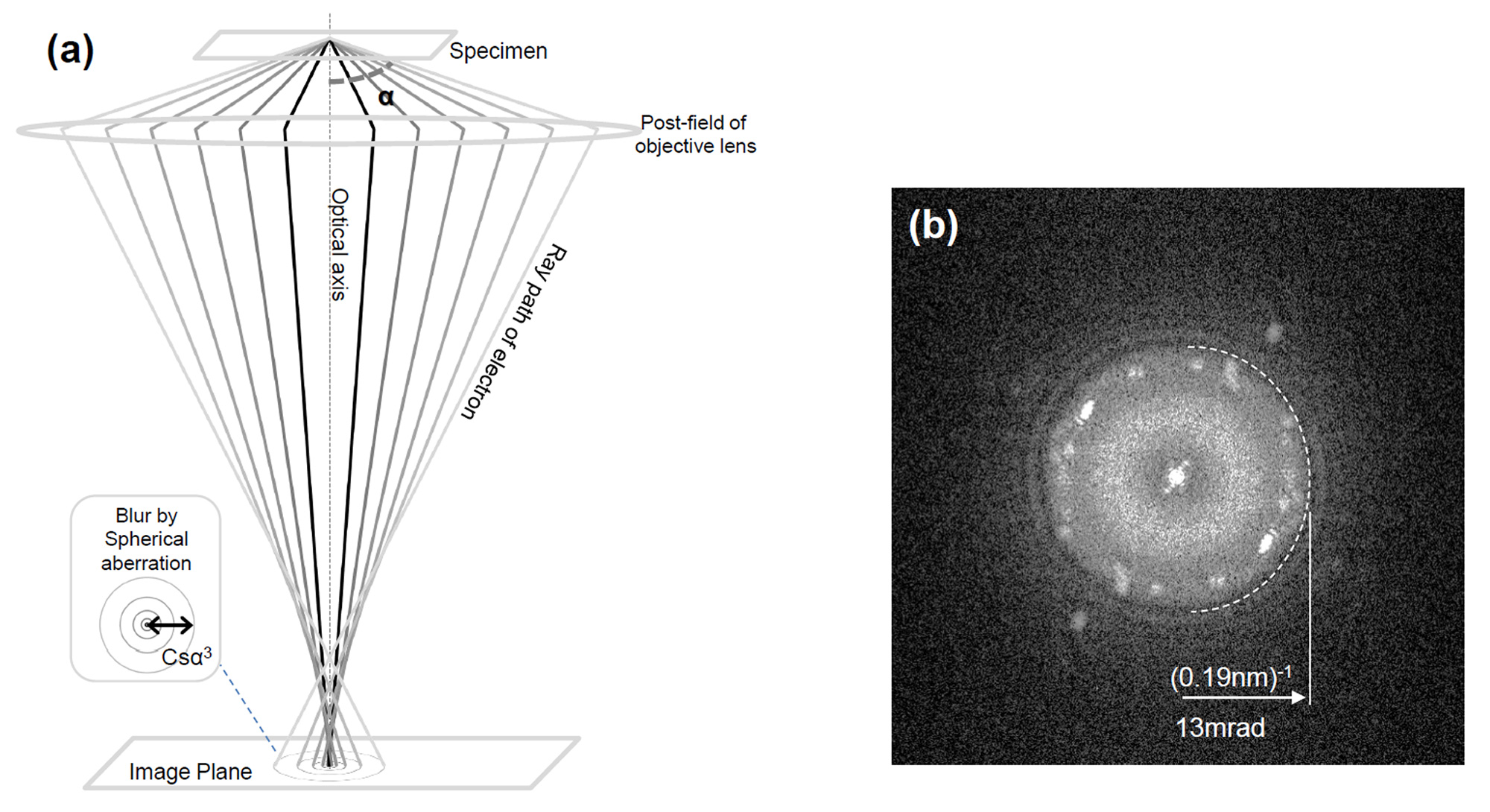
(a) 対物レンズの試料より下方の球面収差を考慮した場合の光線図 (TEMの場合)。試料から射出して光軸に対して角度(α)をもって対物レンズの下方磁場に入射した電子線は、球面収差により (収差の無い場合の電子線と比べて) より強く曲げられる。対物レンズで拡大された像は中間レンズや投影レンズでさらに拡大されてスクリーン上で結像される。試料の一点から射出した電子線はスクリーン上の一点に集束せず、球面収差により広がった像を作る。球面収差による広がりは、試料面上に換算してCsα3で表される (球面収差係数: Cs)。
(b) (3次の) 球面収差係数0.5 mmの対物レンズを用いて、加速電圧200 kVで、シェルツァー・フォーカス (Scherzer defocus) 条件 (球面収差がある場合に最適な分解能を与える条件) で撮影したアモルファス薄膜像のフーリエ変換 (回折) 図形 (Diffractogram)。分解能を決めるFirst Zeroの角度を点線の円弧で示している。
(c) 球面収差を含む結像系で取得したDiffractogram Tableau (Diffractogramの組)。 試料に対して照射電子線を10 mradまで傾けている。傾斜角が大きくなるにつれて球面収差のために各図形は楕円形になるのが分かる。球面収差に対して、Diffractogram Tableauは中心に関して点対称な形状になる。
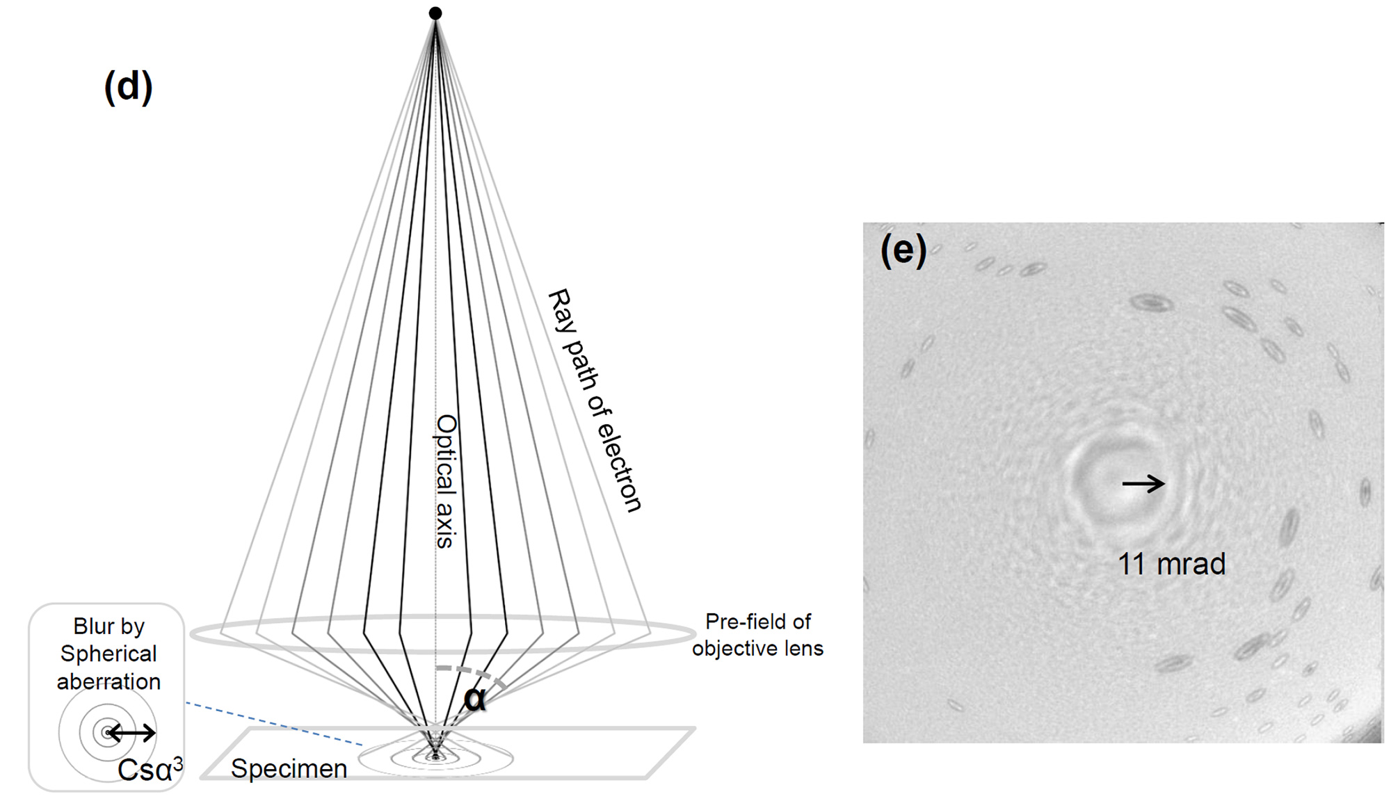
(d) 対物レンズの試料より上方の球面収差を考慮した場合の光線図 (STEMの場合)。STEMでは、電子光源を集束レンズや対物レンズで縮小してnm以下のプローブを作り、スキャンコイルで試料上を走査することにより像を得る。光源から射出して光軸に対して角度(α)をもって対物レンズの上方磁場に入射した電子線は、球面収差により (収差の無い場合の電子線と比べて) より強く曲げられる。そのため、光源の一点から射出した電子線は試料上の一点に集束せず、広がったプローブを作る。プローブの大きさはCsα3 で与えられ、STEM像の分解能が決まる。
(e) (3次の) 球面収差係数0.5 mmの対物レンズを用いて、加速電圧200 kVでアモルファス薄膜から得たRonchigram図形。図形中の中心から一様な強度を持つ角度領域は、電子波の位相がそろった領域を示す (図中の矢印)。この角度内の電子線は、試料上で広がらず、一点に集まる。他方、この角度範囲より外の電子線は試料上で広がりを作る。
The spherical aberration is the third-order geometrical aberration with axial symmetry. Among the geometrical aberrations of the objective lens, the spherical aberration is the most significant aberration to degrade the resolution of high-resolution images. Although the fifth-order and higher-order (odd-order) spherical aberrations exist, only the third-order spherical aberration, which has a significant effect on the image, has been discussed in electron microscopy.
Spread (Blur) of the electron beam due to spherical aberration
When spherical aberration is present, electron beams exiting from the point on the optical axis at the object plane with an angle to the optical axis pass through the lens, do not meet at the point on the optical axis at the ideal image plane, but intersect the optical axis at an upper plane than the ideal image plane (at the lens side). As a result, these electron beams produce a circularly spread image (circular blur) on the ideal image plane. The amount of the spread (blur) is given by the product of the spherical aberration coefficient Cs and cube of the angle α, Csα3 (α is the angle between an electron beam and the optical axis). The value of Cs is always positive for a rotationally symmetric lens with respect to the optical axis.
In the case of TEM
In TEM observation, parallel electron beams are illuminated on a specimen placed near the center of the objective lens. The angular range over which an image is formed with no aberration is limited by the spherical aberration of the post-magnetic field of the objective lens (below the specimen), and the electron beams running at larger angles than the angle for aberration-free imaging produce a spread image (an image blur) on the ideal image plane (Fig.(a)). The angular range with no effect of spherical aberration is given by the position (angle) of the First Zero in the Fourier transformed pattern obtained from a high-magnification TEM image of an amorphous thin-film taken at the Scherzer focus condition. In the example of Fig. (b), the angle of the First Zero is 13 mrad at an accelerating voltage of 200 kV, and the spatial resolution corresponding to the image space is 0.19 nm.
Measurement of spherical aberration
Because of the spherical aberration in the post-field of the objective lens, when the incident electron beam onto the specimen is tilted against the optical axis, two-fold astigmatism and focal shift appear. The larger the tilt angle, the larger the focal shift and two-fold astigmatism. The spherical aberration coefficient Cs can be obtained by measuring the tilt angle dependence on the amounts of the focal shift and two-fold astigmatism. The amount of these aberrations is practically measured using a set of diffractograms (Diffractogram Tableau) (in Fig.(c)), which are taken by varying the tilt and azimuth angles of the electron beam.
In the case of STEM
In STEM observation, a focused electron beam is illuminated onto a specimen placed near the center of the objective lens. Due to the spherical aberration of the pre-field of the objective lens (in front of the specimen), the angular range of the electron beams which meet at a single point on the specimen is limited, and the electron beams with angles larger than the angle for aberration-free probe formation, produce a spread probe (Fig.(d)). The angular region where spherical aberration does not contribute is given as a region of uniform intensity in the electron wave interference pattern (Ronchigram). When acquiring a STEM image, the electron beam is illuminated onto the specimen by selecting the beams of the aberration-free angular region using the condenser aperture. In the example shown in Fig. (e), the angle with no spherical aberration is 11 mrad at an accelerating voltage of 200 kV, and the corresponding probe size in real space is 0.14 nm.
Corrections of the third-order spherical aberration and fifth-order spherical aberration
Nowadays, the (third-order) spherical aberration has been successfully corrected mainly by the use of Cs correctors that combine hexapoles and transfer lenses. After correction of the third-order spherical aberration, the fifth-order spherical aberration is subjected to be corrected at high angles. The Cs correctors mentioned can also correct the fifth-order spherical aberration.
(a) Ray diagram for TEM, where spherical aberration below a specimen placed in the objective lens is taken into account. Electron beams exiting from the specimen and entering into the post-field of the objective lens at an angle α with respect to the optical axis, are more strongly deflected due to the spherical aberration than the electron beams with no aberration. The image magnified by the objective lens is further magnified by the intermediate lens and the projection lens to form the final image on the screen.
The electron beams that exit from a single point on the specimen do not meet at the single point on the screen but create a spread image (image blur) due to spherical aberration. The amount of the image spread is given by Csα3 (Cs: spherical aberration coefficient) in terms of the specimen plane.
(b) Fourier transformed (diffraction) pattern (diffractogram) of an amorphous thin-film image obtained using an objective lens with a (third-order) spherical aberration coefficient Cs of 0.5 mm at an accelerating voltage of 200 kV under the Scherzer focus condition (condition that gives optimum spatial resolution in the presence of spherical aberration). The angle of the First Zero that determines the resolution is indicated by a dotted circular arc.
(c) Diffractogram Tableau (a set of diffractograms) obtained using an imaging system with spherical aberration. The incident electron beam is tilted up to 10 mrad against the specimen. As the tilt angle increases, each pattern becomes more elliptical due to spherical aberration. For spherical aberration, the Diffractogram Tableau is point-symmetric with respect to the center of the Tableau.
(d) Ray diagram for STEM, where spherical aberration above a specimen placed in the objective lens is taken into account. In STEM, the electron source is demagnified by the condenser lens and the objective lens to create a small probe with a size less than 1 nm, and by scanning the probe over the specimen with a scan coil the image of the specimen is formed. Electron beams that exit from the electron source and enter into the pre-field of the objective lens at an angle α with respect to the optical axis, are more strongly deflected due to the spherical aberration than the electron beams with no aberration. That is, the electron beams that exit from a point on the electron source do not meet at a single point on the specimen but create a spread probe. The size of the probe is given by Csα3, which determines the resolution of the STEM image.
(e) Ronchigram pattern of an amorphous thin-film obtained using an objective lens with the (third-order) spherical aberration coefficient Cs of 0.5 mm at an accelerating voltage of 200 kV. The angular region of uniform intensity in the figure indicates the region where the electron waves are in phase (shown by an arrow). The electron beams within this angular range do not spread on the specimen and meet at a single point. On the other hand, the electron beams outside this angular range cause a probe spread on the specimen.
関連用語から探す
説明に「球面収差」が含まれている用語


