シェルツァー・フォーカス
シェルツァー・フォーカス
Scherzer focus
[目次:理論(電子の散乱/回折/結像)]
薄い試料のTEM観察において、結晶構造像を撮影する際に用いられる焦点はずし (デフォーカス) の条件のこと (シェルツァー・デフォーカスともいう) 。対物レンズの球面収差に応じて対物レンズの焦点距離 (焦点はずし量) を調節して、透過波に対する回折波の位相が、できる限り広い空間周波数領域に亘って1/4波長 (位相π/2) ずれるように設定する。
弱位相物体近似が成り立つような薄い試料では、回折波は透過波に対して位相がπ/2ずれている。透過波を実数とすると回折波は虚数になり、そのまま回折波と透過波を干渉させたのではそれぞれの振幅のたし合わせにならず、試料の像を作ることはできない。対物レンズの球面収差に応じて、対物レンズの焦点距離を調整 (焦点はずし) すると、回折波の位相をさらにπ/2 (合計してπ) ずらすことができ、回折波は透過波と同様に実数になる。この回折波を透過波と干渉させると、二つの波の振幅が足し合わされ、試料の像が観察されるようになる。
この焦点はずし量、すなわちシェルツァー・フォーカスdfSchは、球面収差係数CSと電子線の波長λを用いて以下の式で表される [1]。
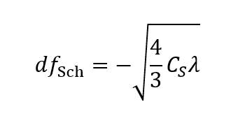
ここで、dfSchの値はマイナスの値である。すなわち、この式はアンダーフォーカス (対物レンズを正焦点より弱くすること) で、構造像が得られることを意味している。焦点はずし量の絶対値は、球面収差係数が大きいほど大きく、電子線の波長が大きいほど (加速電圧が低いほど) 大きくなる。
焦点はずし量をdfSchに設定したとき、位相コントラスト伝達関数の値が最初にゼロになる空間周波数に対応する距離は
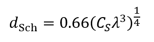
で与えられ、弱位相物体の像の空間分解能 (シェルツァー分解能) という。弱位相物体の像のシェルツァー分解能は、球面収差係数CSの1/4乗と電子の波長λの3/4乗に比例する。そのため、球面収差係数が小さい対物レンズが求められ、波長が短い (加速電圧が高い) 方が像の空間分解能が向上する。
| Accelerating voltage [kV] |
Spherical aberration coefficient [mm] |
Scherzer focus [nm] |
Scherzer resolution [nm] |
|---|---|---|---|
| 100 | 0.5 | -50 | 0.26 |
| 1.0 | -70 | 0.31 | |
| 200 | 0.5 | -41 | 0.20 |
| 1.0 | -58 | 0.23 | |
| 300 | 0.5 | -36 | 0.16 |
| 1.0 | -51 | 0.20 | |
| 1000 | 1.0 | -34 | 0.11 |
表: 典型的な加速電圧に対して、球面収差係数CSが0.5 mmおよび1.0 mmのときの、シェルツァー・フォーカス (デフォーカス量) およびシェルツァー分解能の計算例。通常の加速電圧300 kVの電顕でCS = 0.5 mmの対物レンズを用いた場合は0.16 nmの分解能が得られる。加速電圧が高い1000 kVの場合にはCS = 1.0 mmの対物レンズの場合でも0.11 nmの分解能が得られる。
参考文献
[1] David B. Williams and C. Barry Carter, "Transmission Electron Microscopy: A Textbook for Materials Science", Springer.
(注) なお、球面収差補正装置 (Csコレクター) が搭載されたTEMでは球面収差係数CSをゼロにすることができる。この場合はシェルツァー・フォーカスおよびシェルツァー分解能の式を用いることができない。これらの式はCS≠0を前提として導出されたためである。仮にCS = 0をシェルツァー・フォーカスの式に代入するとdfSch = 0 となり、正焦点では弱位相物体の像を観察することができないはずであるにも拘わらず、正焦点でも結晶構造像が観察可能という結論になってしまう。Csコレクターが搭載されている場合にもコレクターがない場合と同様に、適切なデフォーカスを設定することで結晶構造像が観察できる。しかも、Csコレクターがない場合と比べるとファーストゼロの周波数をかなり高くでき、分解能がより高い試料の構造像を観察できる。また、Csコレクターを搭載したときの分解能は、ファーストゼロの周波数ではなく、電子線の単色性や装置の安定性などで決まることが多い。ちなみに、電界放出型電子銃とCsコレクターを搭載した電子顕微鏡では300 kV以下でも0.1 nmを超える分解能が得られている。
Scherzer focus is the focus condition of the objective lens for forming the crystal structure image of a thin specimen in the TEM mode (also called "Scherzer defocus"). The focal length (defocus amount) of the objective lens is adjusted depending on the spherical aberration of the objective lens so that the phases of the diffracted waves relative to the transmitted wave are shifted by a quarter wavelength (or a phase shift of π/2) over as wide a spatial frequency range as possible.
For a thin specimen for which the weak phase object approximation can be applied, the diffracted waves are out of phase against the transmitted wave by π/2. That is, the transmitted wave takes a real number, each diffracted wave does an imaginary number. As a result, the superposition of the diffracted waves and the transmitted wave does not produce an image of the specimen because the amplitudes of those waves do not add up.
However, by adjusting the focal length (defocus amount) of the objective lens depending on the spherical aberration of the objective lens, the phase of the diffracted wave can be shifted by a further π/2 (π in total). Then, the diffracted waves become real like the transmitted wave. When these diffracted waves are interfered (superposed) with the transmitted wave, the amplitudes of all the waves are added and the image of the specimen is produced.
The amount of defocus or the Scherzer focus dfSch is given by the following equation using the spherical aberration coefficient CS and the electron wavelength λ [1].
The equation indicates that dfSch takes a negative value. This means that, at an underfocus (excitation of the objective lens is weaker than the in-focus), the structure image is obtained. The absolute value of the defocus amount is larger as CS is larger and as the wavelength of the incident electron is larger (as the accelerating voltage is lower).
When the amount of defocus is set to dfSch, the distance corresponding to the spatial frequency at which the value of the phase-contrast transfer function firstly reaches zero, is given by the equation.
dSch is called the spatial resolution of the image of a weak phase object (Scherzer resolution). The Scherzer resolution is proportional to both the 1/4 cube of the spherical aberration coefficient CS and the 3/4 cube of the wavelength λ. Thus, for attaining a high spatial resolution, the objective lens with a small CS is required and a shorter wavelength (higher accelerating voltage) is favored.
| Accelerating voltage [kV] |
Spherical aberration coefficient [mm] |
Scherzer focus [nm] |
Scherzer resolution [nm] |
|---|---|---|---|
| 100 | 0.5 | -50 | 0.26 |
| 1.0 | -70 | 0.31 | |
| 200 | 0.5 | -41 | 0.20 |
| 1.0 | -58 | 0.23 | |
| 300 | 0.5 | -36 | 0.16 |
| 1.0 | -51 | 0.20 | |
| 1000 | 1.0 | -34 | 0.11 |
Table. Examples of the Scherzer focus (defocus amount) and the Scherzer resolution for typical accelerating voltages and for the spherical aberration coefficients CS of 0.5 mm and 1.0 mm.
In the case of a TEM with an ordinary accelerating voltage of 300 kV, the Scherzer resolution is 0.16 nm for CS = 0.5 mm. In the case of a TEM with a high accelerating voltage of 1000 kV, the Scherzer resolution is as high as 0.11 nm even for CS = 1.0 mm.
Reference
[1] David B. Williams and C. Barry Carter, "Transmission Electron Microscopy: A Textbox for Materials Science", Springer.
[Note]
In a TEM equipped with a spherical aberration corrector (Cs corrector), the spherical aberration coefficient Cs can be set to 0 (zero). In such a case, the equations of the Scherzer focus and the Scherzer resolution cannot be used, because these equations are derived with assuming CS ≠0. If CS = 0 is substituted into the Scherzer focus equation, the defocus amount dfSch becomes zero. Although the image of the weak phase object should not be observable at the in-focus, this concludes that the crystal structure image can be observed at the in-focus.
In reality, in the case of a TEM equipped with a Cs corrector, the crystal structure image can be observed by setting the appropriate defocus, as in the case of a TEM without Cs corrector. Moreover, the frequency of the first zero can be considerably higher than without the Cs corrector, or a higher resolution can be attained. It is noted that the resolution of a TEM equipped with a Cs corrector is not determined often by the frequency of the first zero, but by the energy spread of the electron beam and the stability of the microscope instrument (by an envelope function).
For example, in a TEM equipped with a field-emission gun (FEG) and a Cs corrector, a resolution better than 0.1 nm is obtained at an accelerating voltage of even less than 300 kV.
関連用語から探す
説明に「シェルツァー・フォーカス」が含まれている用語


