消衰距離
消衰距離
extinction distance
[目次:理論(電子の散乱/回折/結像)]
消衰距離とは、結晶試料に入射した電子が、侵入深さとともにその強度が強弱を繰り返す周期の距離のことである。
結晶性の試料に電子が入射し、ひとつのブラッグ反射を起こす場合を考える(二波近似という)。入射波(透過波)は格子面で反射され深さとともに減衰する。反射波は深さとともに増大し、ある進入深さt に達すると、入射波の振幅はゼロになり反射波の振幅は最大になる。さらに深さが増すと反射波が透過波の方に向って反射される。深さが2tに達すると、反射波の振幅は再びゼロになり透過波の振幅が最大になる。このように、電子波がその進入深さとともに透過波と反射波の振幅は交互に強弱を繰り返す(動力学的回折における“振り子”解という)。この繰り返しの周期2tを消衰距離ξgと呼ぶ。
消衰距離ξg は ξg= で与えられる。ここで、Vc は結晶の単位胞の体積、λは入射電子の波長、Fgは反射gの結晶構造因子である。
結晶構造因子Fgは、入射電子線に対する結晶の反射能に対応する。そのため、Fg の大きい反射では透過波が反射波に速く移るため、消衰距離が短くなる。すなわち、ξg はFg の大きさに反比例する。また、入射電子線の加速電圧が上がると結晶との相互作用(反射能)が減る。波長が短くなる高加速電圧では、消衰距離は長くなる。すなわち、消衰距離ξgは入射電子線の波長に反比例する。なお、電子線の波長は加速電圧の(1/2)乗に反比例する。
図1に、透過波と反射波が、その進入深さとともに交互に強弱を繰り返す様子を模式的に示した。
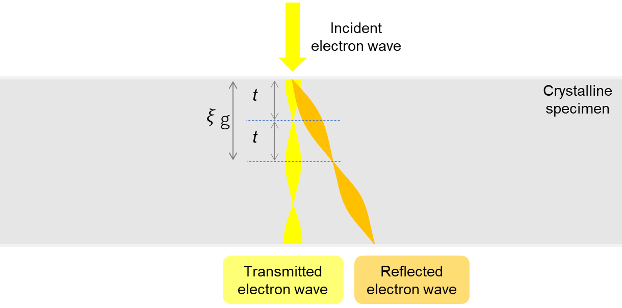
図1:試料内での透過波と反射波の強度変化の模式図。透過波と反射波が試料に対する進入深さとともに、交互に強弱を(消衰距離ξgの周期で)繰り返す。
以下の表は、Al、Si、Cu、Auについての消衰距離の反射指数依存性と加速電圧依存性を示す。結晶構造因子Fgの値は、低次の反射ほど大きく原子番号Zが大きくなると増大するので、ξgは小さくなる。また、加速電圧が高くなると波長は短くなり、ξgは大きくなることを確認できる。消衰距離は、実験的には楔形の結晶を使って等厚干渉縞として観察される。
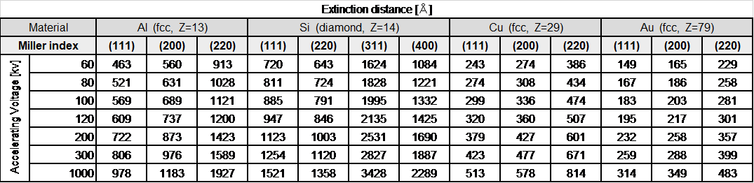
表:Al、Si、Cu、Auに対する消衰距離、“やさしい電子回折と初等結晶学”共立出版より転載
The extinction distance is the distance of a period over which the intensity of electrons incident on a crystalline specimen repeat decrease and increase with the penetration depth.
Consider the case where an electron wave incident on a crystalline specimen causes a single Bragg reflection (called “two-wave approximation”). The incident (transmitted) wave is reflected by a set of crystal lattice planes and damps with the depth of the specimen. The reflected wave increases with the depth. When a certain depth t is reached, the amplitude of the transmitted wave becomes zero and the amplitude of the reflected wave becomes maximum.
As the depth increases further, the reflected wave is reflected toward the transmitted wave. When the depth reaches 2t, the amplitude of the reflected wave becomes zero again and the amplitude of the transmitted wave becomes maximum. In such a manner, the amplitudes of the transmitted and reflected waves alternately decrease and increase with the depth (called “Poendel Loesung” solution in dynamical electron diffraction). The repetition period 2t is termed “extinction distance” ξg.
The extinction distance is expressed by ξg=
. Here, Vc is the unit cell volume of a crystal, λ is the wavelength of an incident electron, and Fg is the crystal structure factor of reflectiong. Since the crystal structure factor Fg corresponds to the reflectivity of reflection g, for a reflection with a larger Fg the transmitted wave is transferred faster to the reflected wave, and then the extinction distance becomes shorter. That is, ξg is inversely proportional to Fg. When the accelerating voltage of the incident electron increases, the interaction between the incident wave and the crystal (or the reflectivity of the crystal) decreases. The extinction distance becomes longer at a higher accelerating voltage or at a shorter wavelength. Thus, the extinction distance ξg is inversely proportional to the wavelength of the incident electron. The wavelength of the electron is inversely proportional to the one-half power of the accelerating voltage.
Fig. 1 illustrates schematically how the transmitted and reflected waves alternate in intensity with the depth of the specimen.
Fig. 1. Schematic of the intensity change of the transmitted and reflected waves in a specimen. The intensities of the transmitted and reflected waves alternately decrease and increase with the depth of the specimen (the repetition period being the extinction distance ξg).
Table below lists the reflection dependence and the accelerating voltage dependence of the extinction distances for Al, Si, Cu and Au. Since the value of the crystal structure factor Fg is larger for lower-order reflections, and is larger for a larger atomic number Z, the corresponding ξg becomes shorter. It is also seen that as the wavelength becomes shorter with the increase of the accelerating voltage, ξg becomes longer.
In experiments, the extinction distance is observed as the equal thickness fringes when using a wedge-shaped crystal.
Table: Extinction distances for Al, Si, Cu and Au.
(reprinted from M. Tanaka, M. Terauchi, K. Tsuda, “Introduction to Electron Diffraction and Elementary Crystallography (in Japanese)”, Kyoritsu Printing Co., Ltd., 2014)
関連用語から探す
説明に「消衰距離」が含まれている用語


