消滅則
消滅則
extinction rule
[目次:理論(電子の散乱/回折/結像)]
禁制反射 (ブラッグ条件を満たしても結晶構造因子がゼロであるために消滅する反射) がどのような場合に起こるかを表す規則を消滅則という。反射の消滅は、1) 空間格子の型によるものと、2) 空間群の対称要素による場合がある。 1) の場合は、運動学的回折が適用される場合にも動力学的回折が適用される場合にも反射は消滅する (図1)。 面心立方格子をとるCuの [001] 入射での電子回折図形の例。面心立方格子では、h, k, l が偶奇混合の場合、結晶構造因子 F(h k l) = 0となり、回折点が消滅する。図では100、110などの回折点が消滅しているのが分かる。JEM-2100Plus (加速電圧 200 kV)で取得。 d-映進面をもつSiの [01-1] 入射での電子回折図形の例。(a) 試料が十分薄い場合と、(b) 試料が厚い場合。d-映進面による反射の消滅は h+k+l = 4n+2 (nは整数) のときに起こる。200反射 (図中に矢印で示す) は禁制反射であるが、遠回り反射、たとえば1-1-1反射 と111反射が引き続いて起こると200反射が現れる。試料が薄い場合 (a) では遠回り反射は弱いので200反射は弱い。試料が厚い場合 (b) では遠回り反射は強くなり200反射の強度は大きくなっている。JEM-F200 (加速電圧 200 kV) で取得。 FeS2の [100] 入射で得た (a) 制限視野回折図形、(b) CBED図形、(c) 入射電子線を [001] 晶帯軸からわずかに傾斜し、100反射を励起して得たCBED図形。 (010) 面に a映進面と a軸に平行に 21 らせん軸があるとする。このとき、h00 の h が奇数の反射は運動学的には消滅するが、動力学効果すなわち遠回り反射によって禁制でなくなり強度を持つ。しかし、遠回り反射を考慮しても、動力学的消滅による暗線が CBEDディスク中に作られる (奇数次の反射の中の暗線)。 東北大学教授 津田健治氏 校閲 田中通義、寺内正己、津田健治、"やさしい電子回折と初等結晶学" (共立出版) p121 M. Tanaka, "International Tables for Crystallography", Vol. B, 2nd online ed., §2.5.3, (International Union of Crystallography, Chester, 2010) M. Tanaka and M. Terauchi, "Convergent Beam Electron Diffraction", (JEOL-Maruzen, Tokyo,1985) p50 (http://www2.tagen.tohoku.ac.jp/lab/terauchi/html/activity/cbedbook.html )
2) の場合は、すなわち空間群の対称要素である映進面や螺旋軸による場合は、運動学的回折が適用されるときにのみ反射の消滅が起こる。動力学効果 (遠回り反射) がある場合は、これらの禁制反射は禁制でなくなり強度を持つ (図2)。しかし、遠回り反射がある場合には特定の入射条件のときには、反射の一部が消滅する。この消滅は、収束電子回折図形で、(運動学的に) 禁制な反射ディスク内に暗い線として現れる (図3、図4)。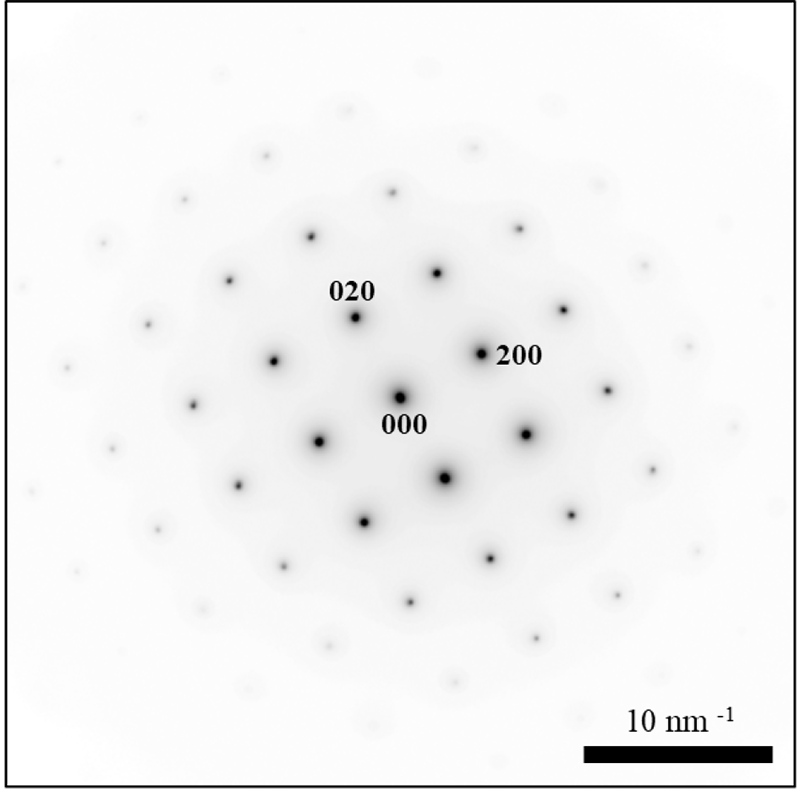
図1 空間格子の型による反射の消滅。
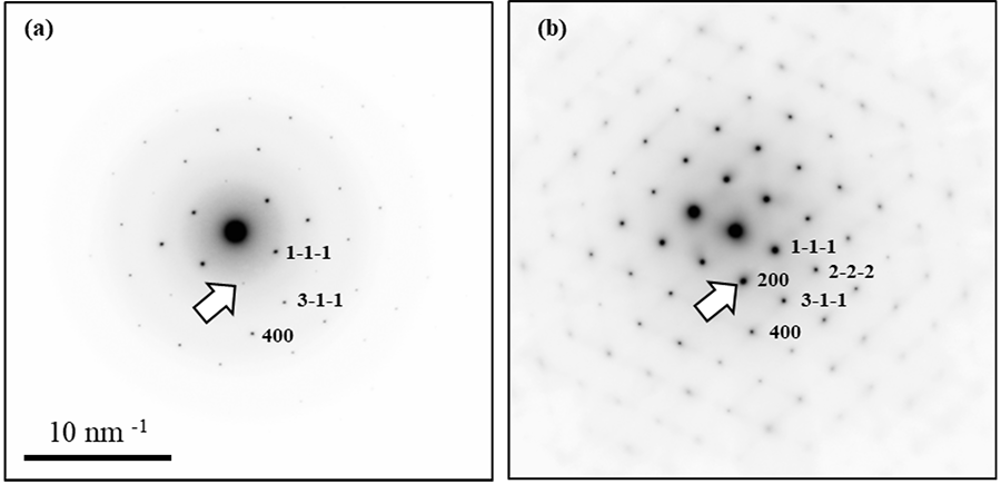
図2 空間群の対称要素(d-映進面)による反射の消滅。
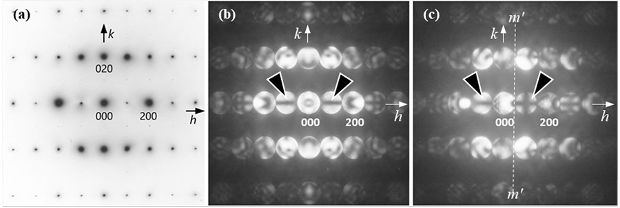
図3 遠回り反射によって励起された反射の部分消滅(暗線)。(東北大学教授 津田健治氏 提供)
FeS2は空間群 P21/a3 に属し、(010) 面に a映進面および a軸に平行に 21 らせん軸がある。これらの対称要素によって奇数次の h00 反射は動力学効果 (遠回り反射) によって強度を持つ。しかし、それらの反射内には動力学的消滅による暗線 (図中矢じりで示す) が作られる。図4の説明を参照のこと。JEM-2010 (加速電圧 100 kV) で取得。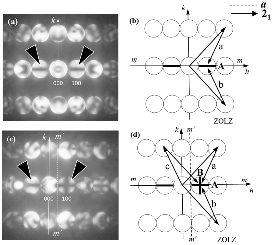
図4 ゼロ次ラウエ帯に属する反射 (ZOLZ反射) を経由する遠回り反射とそれによって CBED 図形中に現れる動力学的消滅 (暗線)。(a), (c) それぞれ、図3(b), (c)の拡大図。(b), (d) 動力学的消滅の説明図。
図 (a) では、奇数次の h00 反射の中に水平方向に暗線Aが見られる。図 (b) に示す遠回り反射経路 a と経路 b は、映進面に対しても、らせん軸に対しても対称な関係になっている。各経路での反射の位相を考慮すると、経路 a と経路 b の反射は互いに打ち消し合い暗線 A を作る。この暗線は全ての奇数次の反射に現れる。
図 (c) は、奇数次の 100 反射をブラッグ条件に合わせた場合で、100 反射内の暗線 A に垂直な暗線 B が見られる。図 (d) に示す遠回り反射経路 a と経路 c が点線 m’-m’ に対称になっており、二つの経路の反射は打ち消し合い、暗線 B が作られる。詳しくは下記の文献を参照のこと。参考文献
The extinction rule means in what case forbidden reflections occur. (Forbidden reflections mean the extinction of reflections due to the crystal structure factor being 0 (zero) even when the Bragg condition is satisfied.) The extinction of the reflections occurs due to the type of the crystal lattice and due to the symmetry element of the space group. In the former case, reflections vanish in both the kinematical diffraction case and the dynamical diffraction case (Fig. 1). In the latter case, i.e. due to glide planes or screw axes (symmetry elements of the space group), the extinction of the reflections occurs only when kinematical diffraction applies. When the dynamical diffraction effect occurs, the forbidden reflections can have certain intensity (Fig. 2). However, when there exists "Umweganregung", an extinction occurs at a part of the reflections under specific beam incidence conditions. The extinction appears as a dark line in kinematically forbidden reflections in a CBED pattern (Figs. 3 and 4). Electron diffraction pattern of Cu taken at the [001] electron incidence, where Cu takes the face-centered cubic lattice. In the case of the face-centered cubic lattice, for the reflections h, k, l having even- and odd-numbered mixed indices, the crystal structure factor takes zero or F (h k l) = 0. Thus, the diffraction spots vanish. In this figure, it is seen that the diffraction spots of 100 and 110, etc., vanish. The pattern was taken with the JEM-2100Plus at an accelerating voltage of 200 kV. Electron diffraction patterns of Si taken at the [01-1] electron incidence, Si crystal having d-glide planes. (a) a sufficiently thin specimen and (b) a thick specimen. Extinction of the reflections due to the d-glide planes occurs when reflection indices take h+k+l = 4n+2 (n is integer). The 200 reflection (indicated by an arrow in Fig. 2(a) and (b)) is forbidden kinematically but has a certain intensity due to "Umweganregung" or successive excitation of the 1-1-1 reflection and the 111 reflection as an example. In the case of a thin specimen (a), "Umweganregung" is weak and thus, the 200 reflection is weak. In the case of the thick specimen (b), "Umweganregung" is strong and thus, the reflection is strong. The patterns were taken with the JEM-F200 at an accelerating voltage of 200 kV. Diffraction patterns of FeS2. (a) a selected-area diffraction pattern taken at the [100] electron incidence, (b) a convergent-beam electron diffraction (CBED) pattern taken at the [100] electron incidence and (c) a CBED pattern taken at the electron incident slightly tilted from the [001] zone axis to excite the 100 reflection. We assume that a-glide planes exist in the (010) planes and 21 screw axes exist parallel to the a-axis. Then, the odd-order h00 reflections vanish kinematically. However, these reflections have certain intensities due to the dynamical diffraction effect ("Umweganregung"). It should be noted that dynamical extinction (dark lines) is produced in the CBED disks excited by "Umweganregung" (dark lines in the odd-order reflections). (Proofread by Professor Kenji Tsuda, Tohoku University) M. Tanaka, M. Terauchi, K, Tsuda, "Introduction to Electron Diffraction and Elementary Crystallography (in Japanese)", (Kyoritsu Printing Co., Ltd.) p121 M. Tanaka, "International Tables for Crystallography", Vol. B, 2nd online ed., §2.5.3, (International Union of Crystallography, Chester, 2010) M. Tanaka and M. Terauchi, "Convergent Beam Electron Diffraction" (JEOL-Maruzen, Tokyo,1985) p50 (http://www2.tagen.tohoku.ac.jp/lab/terauchi/html/activity/cbedbook.html )
Fig. 1. Extinction of reflections due to the type of the crystal lattice.
Fig. 2. Extinction of reflections due to a symmetry (d-glide plane) element of the space group.
Fig. 3. Partial extinction (dark lines) in the reflections excited by "Umweganregung". (Data courtesy: Professor Kenji Tsuda, Tohoku University)
FeS2 belongs to the space group of P21/a3 and has a-glide plane in the (010) plane and 21 screw axis parallel to the a-axis. Owing to these symmetry elements, the odd-order h00 reflections have certain intensities due to the dynamical effect ("Umweganregung"). However in those reflections, dark lines are created due to dynamical extinction (shown by arrowheads in Fig.(b) and (c)). The "dynamical extinction" should be referred to the description in Fig. 4. The patterns were taken with the JEM-2010 at an accelerating voltage of 100 kV.
Fig. 4. "Umweganregung" via the zeroth-order Laue zone reflections (ZOLZ reflections) and dynamical extinction (dark lines) appearing in the CBED patterns. (a), (c) Enlarged figures of Fig. 3 (b), (c). (b), (d) Schematic illustrations of dynamical extinction.
In Fig. (a), the dark line A is seen horizontally in the odd-order h00 reflections. The "Umweganregung" paths a and b, shown in Fig. (b), are symmetric to both the glide plane and the screw axis. Taking account of the phases of the reflections in each path, the resultant reflections passing through the paths a and b cancel out each other, forming the dark line A. The dark line A appears in all the odd-order reflections.
Fig. (c) shows the case where the odd-order 100 reflection satisfies the Bragg condition, exhibiting the single dark line B perpendicular to the dark line A in the 100 reflection. Fig. (d) shows the "Umweganregung" paths a and c. Both the paths are symmetric to the dotted line m’-m’, and the reflections passing through these two paths cancel out each other, forming the dark line B. For more details, refer to the following references.References:
関連用語から探す
説明に「消滅則」が含まれている用語


