体積プラズモン
体積プラズモン
volume plasmon
[目次:分光分析(EELS/EDS/電子構造)]
電子線・荷電粒子線によって金属内で誘起される自由電子の疎密波による集団振動。半導体・絶縁体においても体積プラズモンは誘起される。その振動エネルギー(プラズモンエネルギー)は自由電子密度(半導体・絶縁体のときは価電子密度)の平方根に比例する。体積プラズモンは、電子エネルギー損失分光法(EELS)のスペクトルのピークとして直接観測される。体積プラズモンは縦波なので、横波である光では励起も出来ないし観測も出来ない。
高速電子が金属固体に入射すると、入射電子のクーロン力により、金属中に均一に分布している自由電子に疎密が生じる。誘起された疎密によるクーロン力を駆動力として、自由電子は特定の振動数を持つ縦波振動すなわち固有振動(プラズマ振動)を起こす。この振動を量子化したものを体積プラズモンと呼ぶ。プラズマ振動のエネルギー(プラズモンエネルギー)EPは以下のように表される。
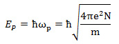
ここで、ωpはプラズマ振動の角振動数。ħ= h ⁄ 2πはプランク定数、eは電子の素電荷、mは電子の質量、Nは自由電子の密度を表す。プラズモンエネルギーは金属内自由電子の密度の平方根に比例する。
プラズモンは本来、金属に対して考えられたものであるが、半導体・絶縁体のように束縛されている電子でも価電子全体の集団振動として励起される。全価電子は原子核および内殻電子からなる正イオンに対して振動する。振動数は価電子密度を上の式に代入して計算される。
⇒図1
(a) 自由電子によるプラズモンの模式図。金属内では、原子核および内殻電子からなる正イオンと自由電子が一様に分布し、全体として電気的に中性の状態にある。そこに外から高速電子が入射すると、そのクーロン力によって自由電子に疎密が生じ、プラスとマイナスの電荷領域が現れる(図1(a)中+と−の領域)。その結果、電場が誘起され(青矢印)、その電場を駆動力として自由電子の集団は固有振動(プラズマ振動)をする。(b)束縛電子によるプラズモンの模式図。赤い点は正イオン、青い丸は価電子を表す。入射電子のクーロン力によって束縛電子(価電子)が変位し、価電子の集団がプラズマ振動をする。図1(b)の上方の矢印は価電子の変位による分極を表す。
束縛電子のプラズマ振動は原子の分極による縦波である。
Alの自由電子密度はN=1.8×10²³ e/cm3である。プラズモンエネルギーは15.7eVと計算され、実験値の15.0eVと良く一致する。LiやNaなどの一価金属でも計算値と実測値は良い一致を示す。
絶縁体であるダイヤモンドでは、価電子密度N=7.0×10²³ e/cm3から求められるプラズモンエネルギーは31eVであり、実験値の34eVと比較的良い一致を示す。LiFやNaClなどのイオン結晶でも、価電子密度から計算したプラズモンエネルギーは実験値をよく再現する。表1に、いろいろな物質に対するプラズモンエネルギーを示す。
ただし、計算で予想されるプラズモンエネルギーと近いエネルギーにバンド間遷移が強く起きる物質では、プラズモンエネルギーが予想値からは大きくずれることがある。銀のプラズモンの場合では、自由電子密度N=0.59×10²³ e/cm3から予想されるプラズモンエネルギーは9.0eVである。
しかし、4.0eVで励起されるd軌道電子のバンド間遷移の影響により、プラズモンピークは3.9eVまで押し下げられる。
⇒Table1. Plasmon energies for several materials
プラズモンは、電子エネルギー損失分光法(EELS)のスペクトルとして実験的に観測される。図2は、EELSで得られたAl、Si、ダイヤモンドのプラズモンによるエネルギー損失スペクトルである。それらのピーク位置は表1の値と良く一致している。Al、Siのスペクトルではそれぞれのプラズモンエネルギー(大きなピーク)の整数倍の位置に弱いピークが観測される。これらは、プラズモンを2回、3回・・・と励起してエネルギー損失したスペクトルである。SiやダイヤモンドのプラズモンピークはAlのピークに比べてピークの幅が広い。これは、プラズマ振動の減衰が大きいことを示しており、価電子がバンド間遷移を起こしてプラズマ振動が崩壊するためである。
(東北大学 佐藤庸平准教授による)
⇒図2
Plasmon peaks of Al, Si and Diamond in EELS spectra
Collective oscillations of free electrons with a longitudinal wave or compressional-wave, which are induced in metals by an electron beam or a charged-particle, are called "volume plasmon". The volume plasmon is excited also in semiconductors and insulators. Its oscillation energy (plasmon energy) is proportional to the square root of the free electron density (valence electron density for semiconductors and insulators). The volume plasmon is directly observed as a peak in an electron energy-loss spectrum. It should be noted that the volume plasmon cannot be excited nor can be observed with a light wave or a transverse wave.
When a high-speed electron beam is incident on a solid metal, the Coulomb force formed by the beam induces a density change (compression) in the homogeneously distributed free electrons in the metal. With the induced Coulomb force as a driving force, a longitudinal oscillation wave of the free electrons with a specific frequency is created (see Fig.1). Quantization of this collective motion of the free electrons is called volume plasmon. The energy of the volume plasmon, EP, is expressed by the following equation.
Here, ωp is the angular frequency of the plasma oscillation. ħ= h/2π is Planck’s constant. e, m, and N respectively express the elementary charge of an electron, the mass of an electron, and the density of the free electrons. The plasmon energy is proportional to the square root of the free electron density in a metal.
Although the volume plasmon is originally considered for free electrons, it is excited also in semiconductors and insulators as a collective oscillation of the whole valence electrons. The valence electrons vibrate collectively against positive ion cores. The energy or frequency of the plasmon is calculated by substituting the density of the valence electrons into the above equation.
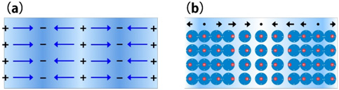
Fig. 1(a) Scematic of plasmon induced by free electrons. Metal is electrically nutral because free electrons and positive ions consisting of an atomic nuclei and inner shell electrons are homogenously distributed. When a high energy electron beam is incident on a metal from outside, the Coulomb force of the incident beam creates a density change in the free electrons, or positive and negative charged regions (indicated by (+) and (−) in Fig. 1(a)). With the electric field (indicated by blue arrows) caused by the density change as a driving force, the free electrons collectively starts a characteristic oscillation (plasma oscillation). (b) Schematic of plasmons of bounded electrons. Red dots and blue circles respectively show positive ions and valence electrons. The bounded valence electrons are displaced by the Coulomb force of the incident electron beam, density changes of the valence electrons being created. Then, the valence electrons collectively oscillate with plasma frequency. Black arrows at the top of Fig. 1(b) represent polarization caused by the displacements of the valence electrons. Plasma vibration of the bounded electrons is a longitudinal wave vibration caused by polarization of the atoms.
The charge density of Al is N = 1.8 × 10²³ e/cm3. The plasmon energy is calculated to be 15.7 eV, showing a good agreement with an experimental value of 15.0 eV. For monovalent metals (Li, Na, etc.), the calculated energies agree well with the energies experimentally obtained.
For diamond (insulator), the plasmon energy is calculated to be 31 eV using the valence electron density (N = 7.0 × 10²³ e/cm3), showing a rather good agreement with an experimental energy of 34 eV. In the cases of ionic crystals such as LiF, NaCl etc., their plasmon energies calculated using the valence electron densities well reproduce the energies experimentally obtained. Table 1 shows the plasmon energies for various materials.
However, for a material in which interband transitions strongly occur close to the expected plasmon energy, the experimental plasmon energy can be largely deviated from the expected energy. For example, in the case of Ag, the plasmon energy expected from the valence electron density of N=0.59×10²³ e/cm3 is 9.0 eV but the experimental plasmon energy is observed at 3.9 eV due to a strong interband transition of the d orbital electrons at 4.0 eV.
Table1. Plasmon energies for several materials
| Materials | Valence electron density [e/cm3] | Ep [eV] (Calculation) | Ep [eV] (Experiment) |
|---|---|---|---|
| Li | 0.47 × 10²³ | 8.0 | 7.1 [1] |
| Na | 0.27 × 10²³ | 6.1 | 5.7 [1] |
| Al | 1.8 × 10²³ | 15.7 | 15.0 |
| Ag | 0.59 × 10²³ | 9.0 | 3.9 |
| Si | 2.0 × 10²³ | 16.5 | 16.7 |
| GaAs | 1.8 × 10²³ | 15.7 | 15.9 |
| Diamond | 7.0 × 10²³ | 31 | 34 |
| LiF | 4.9 × 10²³ | 25.9 | 25.3 [1] |
| NaCl | 1.8 × 10²³ | 15.7 | 15.5 [1] |
[1] H. Raether (1980) "Excitation of Plasmons and Interband Transitions by Electrons" Springer Tracts in Modern Physics, Vol. 88, Springer-Verlag. New York.
(By Associate Professor Yohei Sato, Tohoku University)
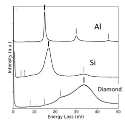
Fig. 2. Plasmon peaks of Al, Si and Diamond in EELS spectra
関連用語から探す
説明に「体積プラズモン」が含まれている用語


