低角度散乱暗視野法
低角度散乱暗視野法
low-angle annular dark-field scanning transmission electron microscopy, LAADF-STEM
[目次:理論(電子の散乱/回折/結像)]
走査透過電子顕微鏡法(STEM)の円環状検出器による暗視野法(ADF)のうち、低‐中角度(25~60mrad)に回折した電子や非弾性散乱電子を円環状の検出器で受け、この電子の積分強度を入射電子プローブの位置に対応させて表示してSTEM像を得る手法。一般には、この手法で得られるSTEM像は回折コントラストや試料の厚さの違いなどが反映される。
HAADF法では、軽元素のみで構成されている分子結晶、二次元結晶、高分子や生物などの有機物の場合、高散乱角での弾性および非弾性散乱電子の強度が弱いためSN比の良い原子分解像が得られない。このような軽元素試料にLAADF法を適用すると、原子番号に依存した高分解能の像をSN比良く得ることができる。
半導体素子(CPUのn-チャンネルMOSFET)の断面薄膜試料のSTEM像 ⇒図
加速電圧: 200 kV、入射電子線の収束角: 半角11 mrad
図(a) HAADF-STEM像。青矢印で示したように、TaやWなど重い元素の存在する部分が明るく観察されている。検出器の取り込み角:半角46 - 208 mrad
図(b) LAADF-STEM像。赤括弧で示した領域中のSiNx層は、青括弧で示したSiO2の領域と比較して、明るく観察されている。この層構造はHAADF像においてほとんど観察することができない。また、赤矢印で示したように格子欠陥も観察されている。検出器の取り込み角:半角14 - 63 mrad
2つの検出器の光線図の比較⇒図
図(a) HAADF-STEMにおける入射電子線の収束角と散乱電子線の検出器への取り込み角の関係。検出器の典型的な取り込み角はβ1 ~ 50 mrad,β2 ~200 mradである。高角度に散乱された非弾性散乱電子を検出する。200 kVの収差補正電子顕微鏡の場合、αは25 mrad程度である。通常、ABF検出器やLAADF検出器はHAADF検出器の下部に配置される。
図(c) LAADF-STEMにおける入射電子線の収束角と散乱電子線の検出器への取り込み角の関係。入射電子線の収束半角をαとすると検出器の取り込み角は、β1はα より少し大きな角度、β2は 60 mrad程度に設定する。回折波と中低角度に散乱された非弾性散乱波を検出する。
Low-angle annular dark-field scanning transmission electron microscopy (LAADF-STEM) is a STEM method which receives diffracted or inelastically scattered electrons at low to medium angles (25 to 60 mrad) using an annular dark-field (ADF) detector. A STEM image is acquired by displaying the integrated intensities of the electrons in synchronism with the incident probe position. It is noted that the LAADF image shows diffraction contrast or difference of specimen thickness dependence.
LAADF-STEM is used in place of HAADF-STEM for a specimen composed only of light elements (molecular crystals, two-dimensional crystals, organic materials like macromolecules, biological materials, etc.). This is because the HAADF image does not have a high signal-to-noise ratio due to weak elastic and inelastic scattering at high angles for such light-element specimens. LAADF-STEM enables us to obtain a high-resolution image with a high signal-to-noise ratio whose intensity depends on the atomic number.
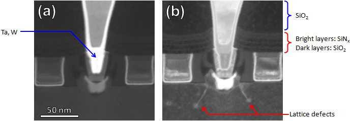
STEM images of the cross-sectional thin film of a semiconductor device (an n-channel MOSFET of CPU). (Accelerating voltage: 200 kV, Convergence semi-angle of the incident electron beam: 11 mrad)
Fig.(a) HAADF-STEM image taken at an acceptance semi-angle of the detector of 46 to 208 mrad. As is shown by a blue arrow, only a region where heavy atoms (Ta, W, etc.) exist are observed with bright contrast.
Fig.(b) LAADF-STEM image taken at an acceptance semi-angle of the detector of 14 to 63 mrad.
SiNx layers in the regions indicated by a red parenthesis are observed brighter than SiO2 regions indicated by a blue parenthesis. Such layer structures are hardly seen in the HAADF image. In addition, the LAADF image also visualizes lattice defects indicated by red allows.
Comparison of Ray diagrams of two detectors
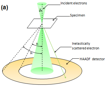 Fig.(a) Relationship between the convergence semi-angle of the incident electron beam and acceptance semi-angles of the detector for HAADF-STEM. Typical inner and outer semi-angles of the detector are respectively β1 = ~50 mrad and β2 = ~200 mrad, detecting inelastically scattered electrons at high angles. The value of the convergence semi-angle α is approximately 25 mrad for a 200 kV Cs-corrected TEM. Usually, an ABF detector and a LAADF detector are placed below a HAADF detector. |
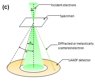 Fig.(c) Relationship between the convergence semi-angle of the incident electron beam and acceptance semi-angles of the detector for LAADF-STEM. The inner and outer acceptance semi-angles of the detector are respectively taken as that β1 is a little larger than α and β2 is ~60 mrad, where α is the convergence semi-angle. It should be noted that the diffracted waves and inelastically scattered electrons over low to medium angles are used for LAADF-STEM. |
関連用語から探す
説明に「低角度散乱暗視野法」が含まれている用語


