電子エネルギー損失分光
電子エネルギー損失分光
electron energy-loss spectroscopy, EELS
[目次:分光分析(EELS/EDS/電子構造)]
入射電子が物質を透過するとき、物質中の電子や原子核とのクーロン相互作用によって散乱されそのエネルギーを一部失う (速度が遅くなる) 電子を非弾性散乱電子という。この電子の損失したエネルギーを分光し、損失スペクトルを得る測定手法を電子エネルギー損失分光 (EELS) 法という。
透過型電子顕微鏡 (TEM) と組み合わせることで、試料物質の微小領域からのエネルギー損失スペクトルを測定することができ、試料の元素の定性・定量分析や誘電的性質 (電子の結合状態) を知ることができる。エネルギー損失の対象となる非弾性散乱 (散乱の素過程) は、格子振動励起 (数十~数百 meV)、価電子励起によるバンド間遷移 (0~10 eV)、自由電子および価電子の集団振動によるプラズモン励起 (10~50 eV)、内殻電子励起 (50 eV~)、である。
損失関数と誘電関数
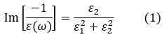
エネルギー損失スペクトルの強度分布は、外部電場の角振動数ωの関数である誘電関数ε(ω)を使って損失関数Im[-1⁄ε(ω)]で表される[1]。 (角振動数ωはħω=ELossで電子線の損失エネルギーと結びついている。) 誘電関数は、角振動数ωの外部電場に対する誘電応答であり、物質の性質を表す固有の関数である。損失関数は、誘電率の実部ε1(ω)と虚部ε2(ω)を使って次式のように表される。
物質に外部振動電場が印加されると、価電子の重心は原子核から変位して電子分極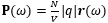 が誘起される。ここで、Nは単位胞中の原子数、Vは単位胞の体積、qは価電子の電荷、r(ω)は価電子の変位ベクトルである。誘電関数と電子分極P(ω)の間には、
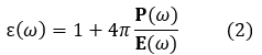
の関係があり、分極P(ω)によって物質定数ε(ω)の値が決まる。価電子の分極振動の減衰はP(ω)の虚数成分として表され、エネルギーの損失は誘電関数の虚数部分に対応する。
価電子励起スペクトル
エネルギー領域0~50 eVのエネルギー損失スペクトルは、価電子励起スペクトルと呼ばれる。このエネルギー領域は、振動数 ωが~1015Hz(E=10~20 eV)の誘電応答に対応する。価電子は共鳴振動を起こして、ε1(ω)は共鳴状態に特有な分散(図1(b))を示す。ε2(ω)が小さく、ε1(ω)がゼロまたは非常に小さい値のとき、損失関数 (1) は大きなピークを示す。このときの振動数ωをプラズマ振動数ωpと呼び、プラズマ振動のエネルギーはE=ħωpと表される。
電子線や荷電粒子線が物質に入射すると、物質内の自由電子または価電子全体が入射電子とのクーロン相互作用によって電荷の疎密波、すなわち縦波振動を励起する。これがプラズモンである。他方、光が物質に入射すると、光は電磁波で横波なので、縦波であるプラズモンを励起することは出来ない。また光によってプラズモンを観測することもできない。光の吸収スペクトルは、価電子の双極子振動の減衰によるエネルギー吸収を表し、誘電関数の虚部ε2(ω)に比例する。
図1(a)にグラファイトの価電子励起スペクトル、図1(b)にグラファイトの誘電関数の実部ε1(ω)(青線)と虚部ε2(ω)(赤線)を示す。図1(a)の27 eVのピークはグラファイトの価電子全体 (すなわちπ電子およびσ電子の合計) の集団による縦波振動でありπ+σプラズモンと呼ばれる。6.5 eVのピークはπ-π*バンド間遷移に起因したピークであり、πプラズモンと呼ばれている。図1(b)に、6.5 eVと27 eVの位置(黒点)でプラズモンの励起条件 ε1(ω)=0が満たされていることを確認できる。さらに、グラファイトの誘電関数の実部 ε1(ω)は、4.2 eVと11.7 eVでπ-π*バンド間遷移、σ-σ*バンド間遷移による共鳴型の分散を示している。そのとき、バンド間遷移によるエネルギーの吸収が起こり、誘電関数の虚部 ε2(ω)にピークを生ずる。しかし、損失関数ではこれらの遷移によるε2(ω)のピークを直接観測することはできない(図1(a))。損失関数から物質の特性を表す誘電関数 ε(ω)を得るには、損失関数にKramers-Kronig変換を施す必要がある[2]。この操作によって得られる誘電関数ε(ω)は、光学的測定で得られる反射率、屈折率、光伝導度などと比較することができる。
実験で得られるスペクトル強度には、プラズモンによるエネルギー損失を複数回起こした多重散乱強度が含まれていることに注意しなければならない。これらの強度はプラズモンエネルギーの整数倍の位置に観測され、試料厚さが増すとその強度は増大する。誘電関数ε(ω)を求めるには一回散乱のみのスペクトル強度を得る必要がある。全スペクトル強度から一回散乱のスペクトル強度を導出には、フーリエ・ログ・デコンボリューション法[2]を用いる。この手法は、n回散乱した非弾性散乱強度がポアソン分布に従い、そのエネルギー分布は1回散乱スペクトル強度のn回のコンボリューションとして表されることに基づいている。また、損失スペクトルに現れる0 eV付近の強度(ゼロロスピーク)は、エネルギーを損失せずに透過した弾性散乱電子であり、測定したスペクトルからゼロロスピークを注意深く差し引かなければならない。ゼロロスピークの差し引き方はスペクトル解析の精度に重要な影響を与える。
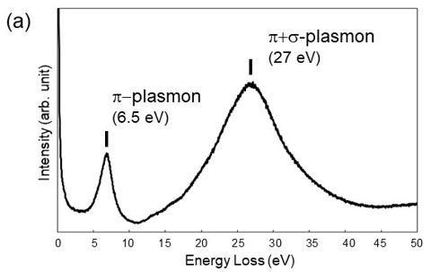
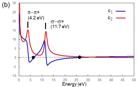
図1:(a)グラファイトの価電子励起スペクトル。6.5 eVのピークはπプラズモン、27 eVのピークはπ+σプラズモンである。(b)グラファイトの誘電関数の実部 ε1(ω) (青線) と虚部 ε2(ω) (赤線)。(b) で、ε1(ω)=0の6.5 eVと27 eVの点 (黒点) はプラズモン励起条件を表し、(a) のEELSスペクトルのピークに対応する。ε2(ω)の4.2 eVと11.7 eVのピークは、それぞれπ-π*バンド間遷移、σ–σ*バンド間遷移によるエネルギー吸収を表す。ただし、これらのピークはEELSでは直接には観測されない。
内殻電子励起スペクトル
エネルギー損失量が50 eV以上のEELSスペクトルを内殻電子励起スペクトルと呼ぶ。このエネルギーに対応する角振動数ω(1016Hz以上)は高周波のため、試料中の価電子はこの振動数ωに追従できず分極は小さくなり、ε1(ω)は~1となる。また、吸収も十分小さくなり ε2(ω)≪1と近似してよい。その結果、損失関数は
と近似でき、光 (X線) の吸収スペクトル (ε2(ω)) と同じ物理量を与える。この領域のエネルギー損失は、内殻電子が伝導帯へ励起されるときのエネルギー吸収で、吸収のエネルギー値から構成元素の定性/定量分析、スペクトルの強度分布から伝導帯の状態密度、電子の結合状態を調べることができる。
炭素材料の電子の結合状態と内殻電子励起スペクトル
グラファイトとダイヤモンドの電子の電子状態の模式図を図2(a)に示す。グラファイト中の炭素原子は、sp2混成軌道によるσ結合とpz軌道によるπ結合を形成している。グラファイト全体では、σ結合軌道(σ)とπ結合軌道(π)は価電子帯を構成する。π反結合軌道(π*)と σ反結合軌道(σ*) は伝導帯を構成している。π軌道による価電子帯とπ*軌道による伝導帯は、僅かに重なり半金属である。
ダイヤモンド中の炭素原子は、sp3混成軌道によるσ結合を形成し、π結合は存在しない。ダイヤモンド全体では、σ軌道は価電子帯を構成し、σ*軌道は伝導帯を構成する。2つの軌道の間には5.5 eVのバンドギャップが存在する。
図2(b)はグラファイトの内殻電子励起スペクトルである。285.5 eVのピークは1s軌道からπ*軌道による伝導帯への遷移に対応し、292 eV~310 eVの強度は1s軌道からσ*軌道による伝導帯への遷移に対応する。πおよびσ結合軌道による価電子帯はすでに電子が占有しているので、1s軌道から価電子帯への遷移は起こらない。291.5 eVのシャープなピーク(▼)は、1s軌道に生成された正孔とσ*軌道へ励起された電子とがクーロン引力によって束縛されている状態、すなわち励起子によるものである。
図2(c)はダイヤモンドの内殻電子励起スペクトルである。その強度分布は1s軌道からσ*軌道による伝導帯への遷移に対応する。ダイヤモンドの結合軌道にπ軌道はなく、伝導帯にπ*軌道が存在しないため、285 eV付近に強度は現れない。289 eVのシャープなピーク(▼)は、1s軌道に生成された正孔とσ*軌道へ励起された電子とのクーロン引力によって束縛された励起子によるものである。ダイヤモンドにはバンドギャップがあることとπ結合がないことから、スペクトル強度立ち上がりの位置(288 eV)はグラファイトのスペクトル強度立ち上がりの位置(284 eV)よりも高エネルギー側で観測される。
このように内殻電子励起スペクトルは、π結合やσ結合すなわち電子の結合状態を明らかにし、さらに伝導帯の状態 (反結合軌道の電子状態) の密度分布を反映する。ただし、EELSは、価電子帯の電子状態を観測することはできない。
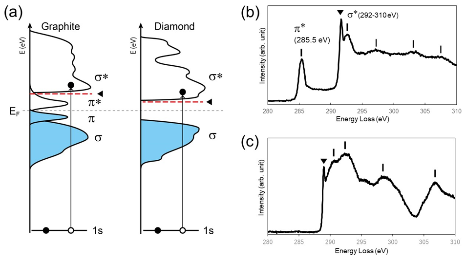
図2:
(a) グラファイトとダイヤモンドの電子構造と1sから2p伝導帯への遷移過程の模式図。
グラファイトの価電子帯 (左図) はπ, σ軌道から成り、伝導帯はπ*, σ*軌道から構成される。ダイヤモンドの価電子帯 (右図) はσ軌道、伝導帯はσ*軌道から構成される。赤い点線は、1s軌道の空孔と励起電子とのクーロン引力によって生じる励起子準位を示す。
(b) グラファイトの内殻電子励起スペクトル。
285.5 eVのピークは1s軌道からπ*伝導帯への遷移に対応する。292 ~ 310 eVは1s軌道からσ*伝導帯への遷移に対応する。291.5 eVのシャープなピーク (▼) は1s軌道から励起子準位への遷移に対応する。
(c) ダイヤモンドの内殻電子励起スペクトル。
288 eVから高エネルギー側の強度は、1sから σ* 伝導帯への遷移に対応する。289 eVのシャープなピーク (▼) は1s軌道から励起子準位への遷移に対応する。
電子エネルギー損失分光法とX線発光分光法
EELS測定は、伝導帯 (非占有状態) の電子状態を観測する手法であり、価電子帯の電子状態を観測することはできない。価電子帯 (占有状態) の電子状態は、電子線を物質に照射することによって放出されるX線をエネルギー分光するX線発光分光法 (X-ray Emission Spectroscopy: XES) によって調べることができる。すなわち、電子線照射によって内殻準位に生じた正孔に、価電子帯から電子が遷移する。その際に放出されるX線を分光することによって得られるXESスペクトルから価電子帯の状態密度分布が得られる。これらの二つの手法を合わせて行うと、伝導帯 (非占有状態) および価電子帯 (占有状態) の両方の電子状態が得られる。
EELS測定装置の現状
高エネルギー分解能EELS測定は、電子線のエネルギーを単色化するモノクロメータと、非弾性散乱電子を分光するアナライザーを搭載したTEMを用いて行われる。汎用型モノクロメータ付きTEMを加速電圧200 kVで作動したとき、約0.2 eV以下のエネルギー分解能のスペクトルを取得できる。近年は、さらに高いエネルギー分解能のEELS測定を行うためのモノクロメータ搭載電子顕微鏡の開発が行われており、数 meVの分解能を達成しているものもある。エネルギー分解能の向上に伴い、測定可能エネルギー領域が赤外領域 (数 meV~0.5 eV) まで拡がり、これまで準弾性散乱電子として扱っていた格子振動による非弾性散乱電子 (数十~数百 meV) の分光が可能になってきている。この性能を生かして、局所領域の格子・分子振動の測定が試みられている。
運動量移送分解EELS (q-EELS)
非弾性散乱電子は、一般には物質中の電子に運動量qを与え (移送し)、入射方向に対して-q方向に散乱される。非弾性散乱電子を単にエネルギー分光するのでなく、運動量移送qの関数として非弾性散乱電子を分光する測定法を運動量移送分解EELS (角度分解EELSまたはq-EELS) 法と呼ぶ。
光による電子遷移はq~0の遷移しか起こせないが、電子線による励起では、光では禁制なq ≠ 0の電子遷移が可能であり、qに依存した価電子励起スペクトルの解析から誘電関数にq依存性も含めた ε(q,ω) を得ることができる。内殻電子励起スペクトルのq依存性を測定すると、反結合軌道(非占有状態)の軌道の方位や伝導帯の状態密度のq依存性などがわかる。
参考文献
[1] H. Raether, Springer Tracts in Modern Physics, 88 (1980), Excitation of Plasmons and Interband Transitions by Electrons (Springer-Verlag Berlin Heidelberg GmbH, 1980)
[2] R.F. Egerton, Electron Energy-Loss Spectroscopy in the Electron Microscope, Third Edition (Springer, 2011)
(東北大学多元物質科学研究所 准教授 佐藤 庸平 執筆)
When the incident electrons pass through a substance, certain electrons are scattered and lose a part of their energies (traveling speed becomes slow) by the Coulomb interactions with the electrons and the atomic nuclei in the substance. These electrons are called inelastically scattered electrons. The spectroscopic method to obtain energy-loss spectra of inelastically scattered electrons is named "electron energy-loss spectroscopy (EELS)."
Combined with transmission electron microscopy (TEM), EELS enables qualitative and quantitative analysis of the constituent elements and measurement of the dielectric properties (bonding states of the electrons) from a micro- or nano-scale specimen (substance) area. Elementary processes of inelastic scattering analyzed by EELS are: (1) excitations of lattice vibrations (a few 10 to a few 100 meV), (2) interband transitions due to valence electron excitations (0 to 10 eV), (3) plasmon excitations due to collective oscillations of free electrons and valence electrons (10 to 50 eV), and (4) inner-shell excitations or core excitations (50 eV or higher).
Energy loss function and dielectric function
The intensity distribution of an energy-loss spectrum is given by the loss function Im[-1⁄ε(ω)], where ε(ω) is the dielectric function, which is a function of the angular frequency ω of an external electric field [1]. (The angular frequency ω is related to the energy loss ELoss of the electron beam by ħω=ELoss.) The dielectric function is the dielectric response of a substance to the external electric field with angular frequency ω, or expresses the dielectric properties of the substance. The loss function is expressed in the following equation using the real part ε1(ω) and the imaginary part ε2(ω) of the dielectric function.
When an external oscillating electric field is applied to the substances, the center of gravity of the valence electrons is displaced from the atomic nucleus and then the electron polarization is induced. Here, N is the number of atoms in a unit cell, V is the volume of a unit cell, q is the electric charge of the valence electrons, and r (ω) is the displacement vector of the valence electrons. The dielectric function is expressed using electron polarization P(ω) as
That is, dielectric function ε(ω) is determined by the electron polarization P(ω). The attenuation of polarized oscillations of the valence electrons is expressed by the imaginary part of P(ω), and thus the energy-loss corresponds to the imaginary part of ε(ω).
Valence-loss spectra
The EELS spectrum in a low energy region (0 to 50 eV) is called the valence-loss spectrum. This energy region corresponds to the dielectric response for the frequency ω = ~1015 Hz (E = 10 to 20 eV), where the valence electrons cause resonant oscillations. ε1(ω) exhibits a spectral distribution specific to a resonant state (Fig. 1(b)). When the value of ε2(ω) is small and ε1(ω) is 0 (zero) or very small, the loss function (1) shows a sharp peak. This frequency ω is called the plasma frequency ωp, and the energy of the plasma oscillation is expressed as E=ħωp.
When an electron beam (or a charged-particle beam) is incident on a substance, the Coulomb interaction of the whole of free electrons or valence electrons in the substance with the incident electron induces a charge-density oscillation or a longitudinal wave oscillation of the electrons of the substance. The longitudinal wave oscillation is called plasmon. On the other hand, when a light wave or an electromagnetic wave is incident on the substance, the plasmon of longitudinal wave oscillation cannot be excited because the light is a transverse wave oscillation. Furthermore, the plasmon cannot be observed by the light wave. An optical absorption spectrum expresses the energy absorption due to the attenuation of the dipole oscillation of valence electrons and the spectrum is proportional to the imaginary part ε2(ω) of the dielectric function.
Fig. 1(a) shows an energy loss spectrum due to valence electron excitations of graphite. Fig. 1(b) shows the real part ε1(ω) (blue line) and the imaginary part ε2(ω) (red line) of the dielectric function of graphite. A spectral peak at 27 eV in Fig. 1(a) is due to the collective longitudinal oscillation of the valence electrons (total of the π electrons and the σ electrons) of graphite, the oscillation being called the π+σ plasmon. A spectral peak at 6.5 eV in Fig. 1(a) is originated from the π-π* interband transition and is called the π plasmon. It is seen in Fig. 1(b) that the plasmon excitation condition ε1(ω) = 0 is satisfied at 6.5 eV and 27 eV (shown with black points).
The real part ε1(ω) of the dielectric function shows the resonance-type dispersion respectively due to the π-π* interband transition at 4.2 eV and due to the σ-σ* interband transition at 11.7 eV. Thereby energy absorption due to the interband transitions or the emergence of a spectral peak of the imaginary part ε2(ω) of the dielectric function takes place. It should be noted that the peaks of ε2(ω) due to the transitions cannot be observed in the loss function (Fig. 1(a)). To obtain the dielectric function ε(ω) representing the characteristic feature of a substance from the loss function, it is needed to apply the Kramers-Kronig transform to the loss function [2]. The dielectric function ε(ω) obtained by the transform can be compared with the results of the optical measurements such as the reflectance, the refractive index, the photo-conductivity.
It should be noted that the spectra experimentally obtained contain the multiple scatterings due to the plasmon. The multiple scatterings are observed at the positions of integral multiples of the plasmon energy. As the specimen thickness increases, their intensities increase. To obtain the dielectric function ε(ω), the spectral intensity of single scattering is needed. The spectral intensity of single scattering can be derived from the spectral intensity experimentally obtained by applying the Fourier-log deconvolution method [2]. The method is based upon the fact that the intensities of n-times inelastic scatterings obey the Poisson distribution and their energy distribution is expressed as n-times convolution of the spectral intensity of single inelastic scattering.
The intensity around 0 eV (zero-loss peak) appearing in the energy-loss spectrum is the contribution of elastically scattered electrons. The zero-loss peak has to be carefully subtracted from the measured spectrum because how to subtract the zero-loss peak contributes greatly to the accuracy of spectroscopic analysis.
Fig. 1(a) Energy loss spectrum due to valence electron excitations of graphite. A spectral peak at 6.5 eV corresponds to the π plasmon and a spectral peak at 27 eV to the π+σ plasmon. (b) The real part ε1(ω) (blue line) and the imaginary part ε2(ω) (red line) of the dielectric function of graphite. In (b), two black points at 6.5 eV and 27 eV show ε1(ω)=0, indicating the plasmon excitation condition. They correspond to two spectral peaks in the EELS spectrum (a). The peaks of ε2(ω) at 4.2 eV and 11.7 eV in (b) exhibit respectively the energy absorption due to the π-π* interband transition and due to the σ–σ* interband transition. It should be noted that these peaks cannot be observed in EELS spectra, as seen in (a).
Core-loss spectra
The EELS spectrum in the high energy region (50 eV or higher) is called the core-loss spectrum. Since the angular frequency ω(1016 Hz or higher) in this energy region is high, the valence electrons cannot follow the frequency ω and then the polarization becomes small or ε1(ω) ~1. The absorption also becomes sufficiently small and then ε2(ω)≪1. As a result, the loss function can be approximated to be
Thus, the loss function in this case gives the same physical quantity as the absorption spectrum (ε2(ω)) of light (X-ray). The energy loss in this energy region corresponds to the energy absorption where the core electron is excited to the conduction band. From the energy values of the absorption spectra, qualitative and quantitative analyses of the constituent elements in the specimen can be performed. From the spectral intensity distribution, the density of states (DOS) of the conduction band and the bonding states of the electrons in the specimen can be investigated.
Bonding states of electrons in carbon materials and their core-loss spectra
Fig. 2(a) shows the schematic of the electronic states of graphite and of diamond. Carbon atoms in graphite form the σ bond due to the sp2 hybrid orbital and the π bond due to the pz orbitals. The valence band of graphite is created by the σ bonding orbitals (σ orbital) and the π bonding orbitals (π orbital). The conduction band is created by the π anti-bonding orbitals (π* orbital) and the σ anti-bonding orbitals (σ* orbital). The valence band due to the π orbitals overlaps slightly with the conduction band due to the π* orbitals, creating a half-metal.
Carbon atoms in diamond form the σ bond due to the sp3 hybrid orbital but does not form the π bond. The valence band of diamond is created by the σ orbitals. The conduction band is created by the σ* orbitals. A band gap with 5.5 eV exists between these two bands. Fig. 2(b) shows a core-loss spectrum of graphite. A spectral peak at 285.5 eV corresponds to the transition from the 1s orbital to the conduction band formed by the π* orbitals. Spectral intensities from 292 to 310 eV correspond to the transitions from the 1s orbital to the conduction band formed by the σ* orbitals. Since the valence band created by the π orbitals and the σ orbitals is already occupied by the electrons, the transition from the 1s orbital to the valence band cannot occur. A sharp peak at 291.5 eV (▼) is attributed to the exciton, which is a bound state of a hole created in the 1s orbital and an electron excited to the σ* orbital by the Coulomb force.
Fig. 2(c) shows a core-loss spectrum of diamond. The intensity distribution corresponds to the transitions from the 1s orbital to the conduction band formed by the σ* orbitals. Since diamond does not have the π orbitals and the π* orbitals, the spectral peak around 285 eV does not appear. A sharp peak at 289 eV (▼) is attributed to the exciton, where a hole created in the 1s orbital and an electron excited to the σ* orbital are bound to each other by the Coulomb force. Since the π bond does not exist but the band gap exists in diamond, the onset energy of the spectral intensity of diamond (at 288 eV) is a little higher than the onset energy of graphite (at 284 eV).
Thus, the core-loss spectrum reveals the bonding states of the electrons or the states of the π* bond and the σ* bond. The intensity distribution in the spectrum is closely related to the state density of the conduction band or the electronic structure of the anti-bonding orbitals. It should be noted that EELS cannot observe the electronic structure of the valence band (occupied states).
Fig. 2 (a) Schematic of the electronic structures of graphite and diamond, and their electron transition processes from the 1s orbital to the 2p conduction band.
In graphite (left figure), its valence band (blue) is composed of the π orbitals and the σ orbitals, and its conduction band is composed of the π* orbitals and the σ* orbitals.
In diamond (right figure), its valence band (blue) is composed of the σ orbitals, and its conduction band is composed of the σ* orbitals.
Red dotted lines indicate the exciton level of graphite and diamond, which is a bound state between a hole created in the 1s orbital and an excited electron by the Coulomb force.
(b) Core-loss spectrum of graphite. A spectral peak at 285.5 eV corresponds to the transition from the 1s orbital to the π* conduction band. The spectral intensities between 292 eV and 310 eV correspond to the transitions from the 1s orbital to the σ* conduction band. A sharp peak at 291.5 eV (▼) corresponds to the transition from the 1s orbital to the exciton level.
(c) Core-loss spectrum of diamond. The spectral intensities from 288 eV to 310 eV correspond to the transitions from the 1s orbital to the σ* conduction band. A sharp peak at 289 eV (▼) corresponds to the transition from the 1s orbital to the exciton level.
Comparison between EELS and XES
EELS is a method to investigate the electronic structure of the conduction band (unoccupied states), but cannot obtain that of the valence band (occupied states). The electronic structure of the valence band can be investigated by X-ray emission spectroscopy (XES), which is a spectroscopic method to measure the X-ray emission spectrum generated by irradiating a specimen with an electron beam. That is, when the electron beam is incident on the specimen, the electron in an inner shell is emitted and a hole is created there. Then, an electron of the valence band falls to the hole and X-ray emission occurs at this transition. The XES spectrum acquired enables us to obtain the density of states (DOS) of the valence band. Combined analysis with EELS and XES provides the electronic structures of both the conduction band (unoccupied states) and the valence band (occupied states).
Current status of EELS instruments
High energy-resolution EELS measurement is performed using a TEM equipped with a monochromator to monochromatize the energy of the incident electron beam and with an energy analyzer to obtain spectra of inelastically scattered electrons. When a TEM equipped with a monochromator of commercial type is used at an accelerating voltage of 200 kV, EELS spectra with an energy-resolution of 0.2 eV or better can be acquired. Nowadays, the TEMs incorporating a monochromator which enables superbly high energy-resolution are being developed. Some instruments have achieved a few meV energy resolution. With an improved energy resolution, the measurable energy region by EELS has extended to the infrared region (a few meV to 0.5 eV), thus enabling spectroscopic analysis of inelastically scattered electrons due to lattice vibrations (a few 10 to a few 100 meV), which have been treated as quasi-elastically scattered electrons. Taking advantage of such high performance, measurements of lattice and molecular vibrations in local areas have been conducted by EELS.
Momentum transfer resolved EELS (q-EELS)
Inelastically scattered electrons give a momentum q to the electrons in a substance and are scattered in the direction -q against the incident-beam. A method to obtain the energy loss spectra of the inelastically scattered electrons as a function of momentum transfer q, rather than to obtain simply energy loss spectra, is called the momentum transfer resolved EELS (angle resolved EELS or q-EELS) method.
The electron transition by a light beam causes only the transition of q ~0, but the electron excitation by an electron beam allows the transitions of q ≠ 0. Thus, when an electron beam is incident on a substance, the dielectric function ε(q,ω) which takes account of the q dependence of the dielectric function can be obtained from the analysis of the q dependent valence-loss spectra. Measurement of the q dependent core-loss spectra reveals the q dependence of DOS of the conduction band and the orientation of the anti-bonding orbitals (unoccupied states).
References
[1] H. Raether, Springer Tracts in Modern Physics, 88 (1980), Excitation of Plasmons and Interband Transitions by Electrons (Springer-Verlag Berlin Heidelberg GmbH, 1980)
[2] R.F. Egerton, Electron Energy-Loss Spectroscopy in the Electron Microscope, Third Edition (Springer, 2011)
(By Associate Professor Yohei Sato, Tohoku University)
関連用語から探す
説明に「電子エネルギー損失分光」が含まれている用語


