偏析
偏析
segregation
[目次:結晶等(結晶構造/材料試料)]
金属、セラミックス、高分子などの材料中に含まれる成分元素の一部が不均一に凝集する現象。金属材料の場合、熱処理後の冷却過程や時効処理の際にしばしば起きる。偏析は、材料の機械強度、電気特性などに影響を及ぼす。
図1, 2は、Al-Mg-Si-Cu合金の偏析 (Q'相) をTEM暗視野像、制限視野電子回折図形およびHAADF-STEM像とEDSによる元素分布像で解析した例。TEM暗視野像では、析出物由来の回折スポットを選択することで析出物の分布を可視化できる。制限視野電子回折図形からは、偏析に由来する反射が分かる。強いスポットは母相のAl由来の反射であり、強いスポットの周りに存在する弱いスポットは添加元素の偏析による反射である。HAADF-STEM像ではQ'相の構造を直接観察できる。EDS分布像からSi, Mg, Cuなどの添加元素の分布が分かる。
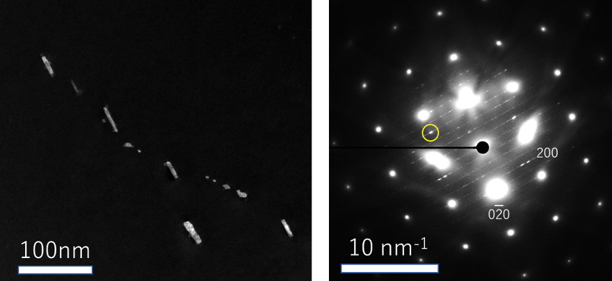
図1 Al-Mg-Si-Cu合金のTEM暗視野像 (電子回折図形中の黄色で示すスポットを選択) (左図) と制限視野電子回折図形 (右図)。偏析の分布状態が分かる。
加速電圧200 kV、[001]入射
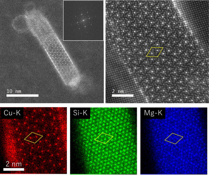
図2 (上段) Al-Mg-Si-Cu合金のQ'相のHAADF-STEM像 (左: 全体像とFFTパターン、右: 一部拡大) : (下段) EDS元素分布像 (Cu: 赤、Si: 緑、Mg: 青の元素分布を示す)
観察装置: JEM-ARM200F、薄膜試料作製: JIB-4700F
A phenomenon where a part of the constituent elements in a material (metals, ceramics, high polymers, etc.) aggregates unevenly. In the case of a metal, segregation often occurs at a cooling process after a heat treatment or at an aging treatment. Segregation affects the mechanical strength and electrical properties of materials.
Figs 1 and 2 show an example of the segregation (Q' phase) of an Al-Mg-Si-Cu alloy analyzed by a TEM dark-field image, a selected-area diffraction (SAD) pattern, HAADF-STEM mages and EDS elemental-mapping images. In the TEM dark-field image, the distribution of the precipitates is visualized by selecting a diffraction spot originated from the precipitates. In the SAD pattern, the reflections originated from segregation are identified. The strong spots seen in the pattern correspond to the reflections from Al in the matrix phase while the weak spots around the strong spots correspond to the reflections due to the segregation of the added elements. In the HAADF-STEM images, the structure of the Q' phase is directly seen. From the EDS elemental-mapping images, the distribution of the added elements of Si, Mg and Cu are revealed.
Fig. 1 TEM dark-field image (left) of an Al-Mg-Si-Cu alloy (taken from a spot indicated by a yellow circle in the right electron diffraction pattern) and the selected-area diffraction (SAD) pattern (right). The distribution state of the segregation is revealed.
Accelerating voltage: 200 kV, [001] incidence.
Fig. 2 (Top) HAADF-STEM images of the Q' phase of an Al-Mg-Si-Cu alloy (left: whole image and the FFT pattern, right: partially enlarged).
(Bottom) EDS elemental-mapping images (elemental distribution of Cu (red), Si (green) and Mg (blue), from left to right).
Instrument for taking images: JEM-ARM200F. Instrument for thin-film preparation: JIB-4700F.
関連用語から探す
説明に「偏析」が含まれている用語


