粒界
粒界
grain boundary
[目次:結晶等(結晶構造/材料試料)]
多結晶固体における各結晶粒どうしの境界のこと。結晶粒界ともいう。
grain boundary ⇒図
シリコン多結晶の高分解能HAADF-STEM像。加速電圧:300kV。
図中の赤色矢印で示した境界がシリコン結晶の粒界であり、ダンベル構造の向きが変化しているのが分かる。
この場合、粒界はΣ3, [110]/{111}と表記される。
"Grain boundary" separates respective crystalline particles with different orientations in a polycrystalline solid. Grain boundaries are also called crystalline grain boundaries.
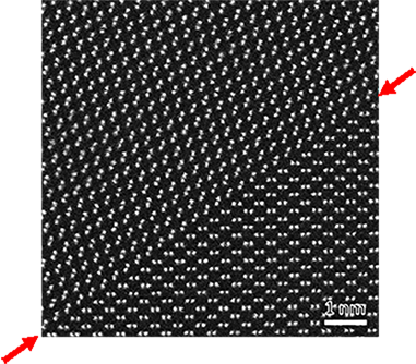
High-resolution HAADF-STEM image of polycrystalline silicon taken at an accelerating voltage of 300 kV. The boundary indicated by red allows is a grain boundary of crystalline silicon. The image reveals that the dumbbells of silicon atoms change their orientations across the boundary. This grain boundary is expressed by Σ3, [110]/{111}.
関連用語から探す
説明に「粒界」が含まれている用語


