微分位相コントラストイメージング
微分位相コントラストイメージング
differential phase contrast imaging
[目次:理論(電子の散乱/回折/結像)]
試料中の電磁場による電子ビームの偏向を各スキャン点で計測し、電磁場を可視化、画像化するSTEM法の一種。試料の電磁場によるビームの偏向を計測するためには分割型検出器やピクセル型検出器が用いられる。分割型検出器では、図のように対向する検出器同士の信号量の差分を取ることにより、試料内でのビームの偏向量(検出器上でのビームの移動量)とその方向を検出する。
電子ビームが偏向されると、電子波は電子ビームの偏向量に比例した位相変化を受ける。この位相変化(傾き)は、言い換えれば位相の微分なので、微分位相コントラストという名称が付けられている。微分位相コントラストイメージングは、ミクロンオーダーからナノメートルオーダーの磁区観察に活用されている。昨今では電場解析にも用いられ、球面収差補正装置が搭載された顕微鏡では、原子分解能レベルでの電場観察が報告されている。
分割検出器の模式図⇒図
図(a) 試料による電子線の偏向を、分割型検出器を使って検出するときの模式図(試料によって電子ビームが偏向されていない場合)。
この例ではSTEM検出器は四分割されている。検出器にはコンデンサー絞りの影が投影される。
図(b) 図(a)を、入射電子線の上方から見た図。四分割されたそれぞれの検出器に入る信号量は同じなので、対向する検出器同士の信号量の差分はゼロになる。
図(c) 試料による電子線の偏向を、分割型検出器を使って検出するときの模式図(試料によって電子ビームが偏向されている場合)。
図(d) 図(c)を、入射電子線の上方から見た図。 x の正方向にビームが偏向されている場合、検出器1で受ける信号量(Idet1)から検出器3の信号量(Idet3)を引いた量は負になるが、検出器2 (Idet2)と検出器4 (Idet4)の差分はゼロのままである。これにより、ビームが x の正方向に偏向されたことを知ることができ、また差分の絶対値から偏向量を計算することができる。
Differential phase contrast imaging is a STEM method to visualize an electromagnetic field in a specimen by measuring the deflection of an electron beam due to the field at each beam-scan point. The beam deflection is measured with a segmented detector or a pixelated detector. When a segmented detector composed of four segments is used (see Figure below), the angle and the direction of the beam deflection (beam shift on the detector plane) are measured from the difference between the signal amounts acquired with the two segments opposed to each other.
It is noted that the naming “differential phase contrast” of this imaging method is originated from that the deflection of the electron beam causes the differential or gradient of the phase of the electron wave.
Differential phase contrast imaging is utilized for observations of micrometer to nanometer scale magnetic domains. In recent years, this imaging method has been applied to analysis of electric fields, and the electric field at the atomic scale has been observed using a transmission electron microscope equipped with a Cs corrector.
Schematics of a segmented detector 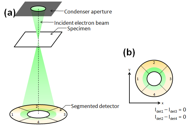
Fig.(a) Schematic of detection of the electron beam deflection in a specimen using a segmented detector (In case that the electron beam is not deflected by the specimen).
Fig.(b) A STEM detector in this case is composed of four segments. The shadow of the condenser aperture is projected onto the detector.Top view of the detector and the electron beam seen along the incident beam direction. The signal amounts are the same for the four segments. Thus, there is no difference between the signal amounts acquired from the two segments opposed to each other.
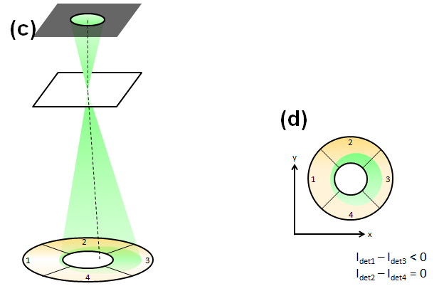
Fig.(c) Schematic of detection of the electron beam deflection in a specimen using a segmented detector (In case that the electron beam is deflected by a specimen).
Fig.(d) Top view of the detector and the electron beam seen along the incident beam direction. When the beam is deflected in the positive direction of the x axis, the signal amounts obtained by subtracting Idet3 from Idet1 becomes a negative value, whereas there is no difference between the signal amounts Ide2 and Idet4. As a result, the beam is found to be deflected in the positive direction of the x axis, and the deflection angle is measured from the absolute value of the signal difference.
説明に「微分位相コントラストイメージング」が含まれている用語


