エキシトン
エキシトン
Exciton
[目次:分光分析(EELS/EDS/電子構造)]
光または電子線によって固体内の電子が励起されると、占有電子状態に正孔が生じる。正孔は正の電荷とみなされる。励起された電子と正孔はクーロン引力によってお互いに引きつけ合い、電子—正孔対を形成する。これをエキシトンと呼ぶ。エキシトンの正孔と電子は、固体中でお互いに一定の距離を保ちながら周回している状態にある。このときのエキシトンは、伝導帯の最低エネルギー準位よりも数十~数百meV低いエネルギー位置にエネルギー幅の狭いエネルギー準位を形成する。この準位は、電子エネルギー損失スペクトルの立ち上がり位置の付近にシャープなピークとして観測される。
図1(a)にダイヤモンドの内殻電子励起スペクトルを示す。このスペクトルは、ダイヤモンドの1s内殻準位から伝導帯への遷移に対応し、伝導帯の状態密度(DOS)分布を表す。289 eVに観測されるシャープなピーク(▼)がエキシトンピークである。ダイヤモンドの電子状態の模式図を図1(b)に示す。1s内殻準位にできた正孔と励起された電子とでエキシトンが形成される。このとき、エキシトンの大きさ(直径)は0.1 nm程度である。ダイヤモンドのエキシトンの電子準位は、伝導帯の最低エネルギー準位よりも約0.2 eV低い位置に形成される(図1(b)赤点線)。
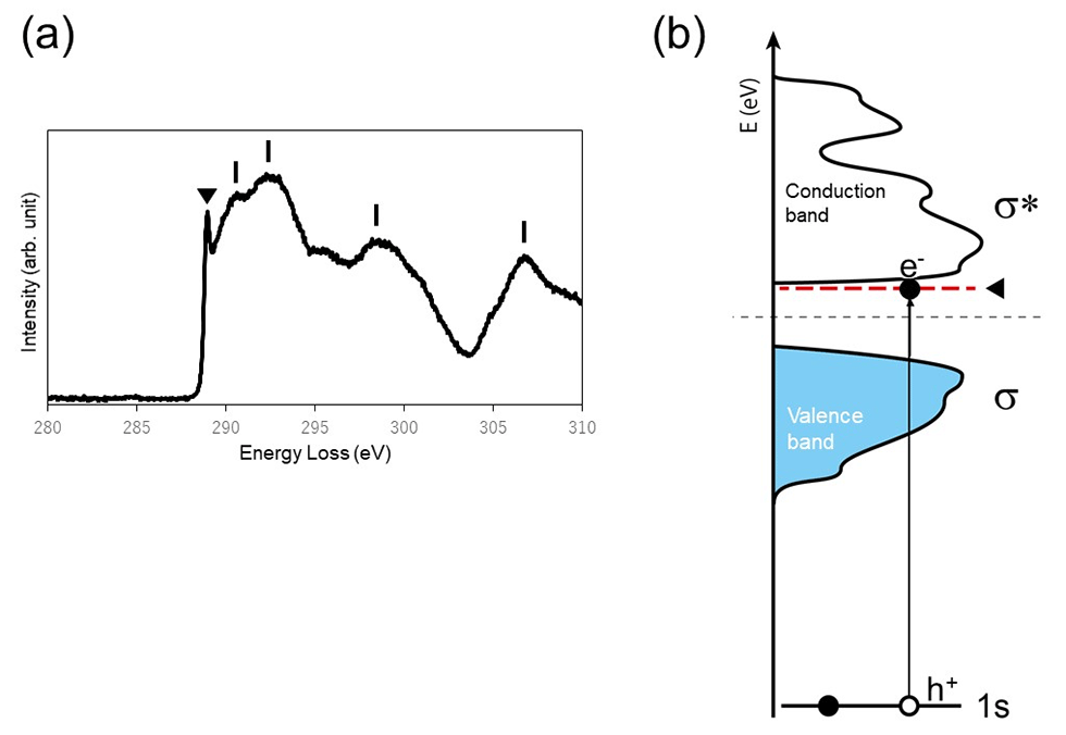
図1(a)ダイヤモンドの内殻電子励起スペクトル。289 eVのシャープなピーク(▼)がエキシトンピークである。それに続く高エネルギー側のスペクトルの強度分布は、ダイヤモンドの伝導帯のDOSを表す。(b)ダイヤモンドの電子状態の模式図。電子線によって1s内殻軌道電子が励起され(e-)、1s軌道に正孔が生ずる(h+)。励起された電子は、その正孔と引き合い、ダイヤモンドの伝導帯の最低エネルギー準位よりも約0.2 eV低い位置にエキシトン準位 (赤点線) を形成する。
図2(a)にSiO2の価電子励起スペクトルを示す。SiO2のバンドギャップエネルギー(~9 eV)付近に観測されるスペクトルの強度立ち上がりは、価電子帯の最高エネルギー準位から伝導帯の最低エネルギー準位への遷移に対応する。この強度の立ち上がり位置の直上すぐ高エネルギー側(10.4 eV)に見られるピーク(図2 (a)▼印)がエキシトンピークである。図2(b)にSiO2の電子状態の模式図を示す。価電子帯にできた正孔と励起された電子の間でエキシトンが形成される。この場合のエキシトンは、図1(a)に示したエキシトンよりもクーロン引力が弱く、空間的に直径が数nm程度広がっている。そのために、エキシトンのエネルギー準位は伝導帯の底部に形成される(図2(b))。さらに、SiO2内のエキシトンは数十~数百nmの範囲に拡散し、拡散中に再結合して消滅することもある。
注意する点として、価電子励起スペクトル(図2(a))は損失関数であって、図1(a)に示したような誘電関数の虚部ではないことである。したがって、エキシトンの電子準位の正確な値は、Kramers-Kronig解析を用いて損失関数から誘電関数を導出し、誘電関数の虚部のピークエネルギーから求める必要がある。しかし、観測された損失関数でのSiO2のエキシトンピークは十分にシャープなため、誘電関数の虚部に表れるピーク位置とほぼ同じになる。
(東北大学多元物質科学研究所 准教授 佐藤庸平 執筆)
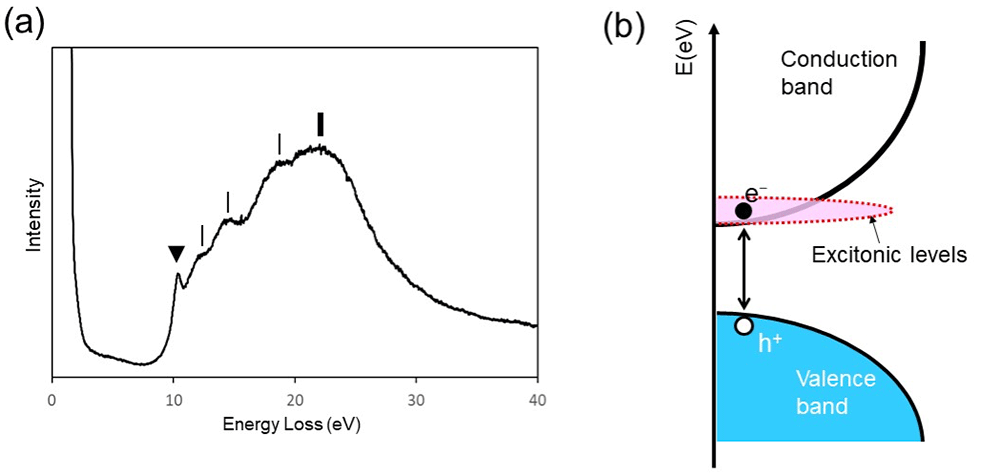
図2(a)SiO2の価電子励起スペクトル。10.4 eVのピーク(▼)がエキシトンピークである。22 eVのピーク(縦太線)は、SiO2の価電子全体の集団振動によるプラズモンピークである。その他のスペクトル構造(縦細線)はバンド間遷移によって生じる構造である。(b)SiO2の電子状態の模式図。励起された電子(e-)は、価電子帯に生成された正孔(h+)と弱く結合し、伝導帯の底部にエキシトン準位((b)赤い領域)を形成する。
Consider a state in which an electron in a solid is excited and a hole is created where the electron was occupied by a light beam or an electron beam. This hole is positively charged. The excited electron and the created hole are attracted to each other by the Coulomb force, forming an electron-hole pair. This is called the exciton. The hole and electron forming the exciton make a circular orbital in the solid while maintaining a certain distance from each other. The exciton forms an energy level with a narrow energy width at an energy position of tens to hundreds of meV below the lowest energy level of the conduction band. This energy level is observed as a sharp peak near the onset energy position of an electron energy-loss (EELS) spectrum. Fig. 1 (a) shows a core-loss spectrum of diamond. This spectrum corresponds to the transition from the 1s core-level to the conduction band of diamond, and exhibits the density of states (DOS) distribution of the conduction band. A sharp peak observed at 289 eV (▼) is the exciton peak.
Fig. 1 (b) shows the schematic of the electronic structure of diamond. The exciton is formed by the hole created in the 1s core-level and the excited electron. In this case, the size (diameter) of the exciton is around 0.1 nm. The energy level of the exciton of diamond is formed at about 0.2 eV below the lowest energy level of the conduction band (indicated by a red dotted line in Fig. 1 (b) ).
Fig. 1(a) Core-loss spectrum of diamond. A sharp peak at 289 eV (▼) is the exciton peak. The spectral intensity distribution extending from the exciton peak at the high energy side exhibits the DOS of the conduction band. (b) Schematic of the electronic structure of diamond. The electron beam excites an electron (e-) in the 1s core-orbital to create the hole (h+) in the 1s orbital. The excited electron is attracted to the hole with the positive charge, forming the exciton level (red dotted line) at about 0.2 eV below the lowest energy level of the conduction band of diamond.
Fig. 2(a) shows a valence-loss spectrum of SiO2. The onset of the spectrum observed near the band gap energy (~9 eV) of SiO2 corresponds to the transition from the highest energy level in the valence band to the lowest energy level in the conduction band. A spectral peak (▼) in Fig. 2(a)) observed just above the onset energy is the exciton peak. The schematic of the electronic structure of SiO2 is shown in Fig. 2(b). The exciton is formed by the hole created in the valence band and the excited electron. The exciton in this case spatially is spread to a size (diameter) of a few nm in diameter because the Coulomb force is weaker than the case of Fig. 1. Then, the energy level of the exciton (shown by pink in Fig. 2(b)) is formed at the bottom of the conduction band. In addition, the exciton in SiO2 can move in the range of tens to hundreds of nm by diffusion and can recombine and disappear during diffusion.
It is important to note that the valence-loss spectrum of Fig. 2(a) is the loss function but not the imaginary part of the dielectric function as shown in Fig. 1(a). Thus, the accurate value of the energy of exciton has to be obtained from the peak energy of the imaginary part of the dielectric function by deriving the dielectric function from the loss function using Kramers-Kroning analysis. However, the exciton peak of SiO2 observed in the loss function is sufficiently sharp and almost identical to the energy position appearing in the imaginary part of the dielectric function.
(By Associate Professor Yohei Sato, Tohoku University)
Fig. 2(a) Valence-loss spectrum of SiO2. A spectral peak at 10.4 eV (▼) is the exciton peak. A peak at 22 eV (bold vertical line) is the volume plasmon peak due to collective oscillations of the whole valence electrons of SiO2. The other spectral structures (fine vertical lines) are originated from interband transitions. (b) Schematic of the electronic structure of SiO2. The excited electron (e-) is bounded weakly with the hole (h+) created in the valence band. As a result, the energy level of the exciton (shown by pink in (b)) is formed at the bottom of the conduction band of SiO2.
関連用語から探す
説明に「エキシトン」が含まれている用語


