YAG反射電子検出器
YAG反射電子検出器
YAG backscattered electron detector, YAG BSE detector, YAG BED
[目次:装置]
イットリウム・アルミニウム・ガーネット(Yttrium Aluminum Garnet(Y3Al5O12); 略称YAG)と呼ばれる結晶に、蛍光活性物質としてセリウム(Ce)を添加したCe:YAGを用いた反射電子検出器。
最も広く使われる反射電子検出器は半導体反射電子検出器であるが、応答時間が長い(応答速度が遅い)ため速い走査速度で試料を観察したとき試料の像がぼける。この現象を避けたいときにYAG反射電子検出器が用いられる。
図1のように、集束電子線を試料に照射した際に発生する反射電子を試料の直上に設置したCe:YAGに当てることで発生する光(蛍光)を、ライトガイドを介して光電子増倍管に導き、光電陰極で光を電子に変換し、さらに電子を増倍する。増倍された電子は陽極に到達し、接続された電気回路にて電圧信号に変換され増幅される。Ce:YAGは蛍光減衰時間が短いことから(70 ns程度)、半導体反射電子検出器と比較して一桁以上応答時間が短い。
半導体反射電子検出器のように応答時間が長い場合、速い走査速度で観察したときに試料が横に動いたようなぼけた画像になることがある(図2左下のSEM像)。YAG反射電子検出器は応答時間が短く、速い走査速度でも画像がぼけずに観察できる。そのため、試料ステージを素早く動かしても像を明瞭に見ることができ、目的の観察位置をタイムラグなく見つけることができる。またアレイトモグラフィーのように広範囲にわたって多くの像を撮影する場合に、画像の取得時間を短縮できる。
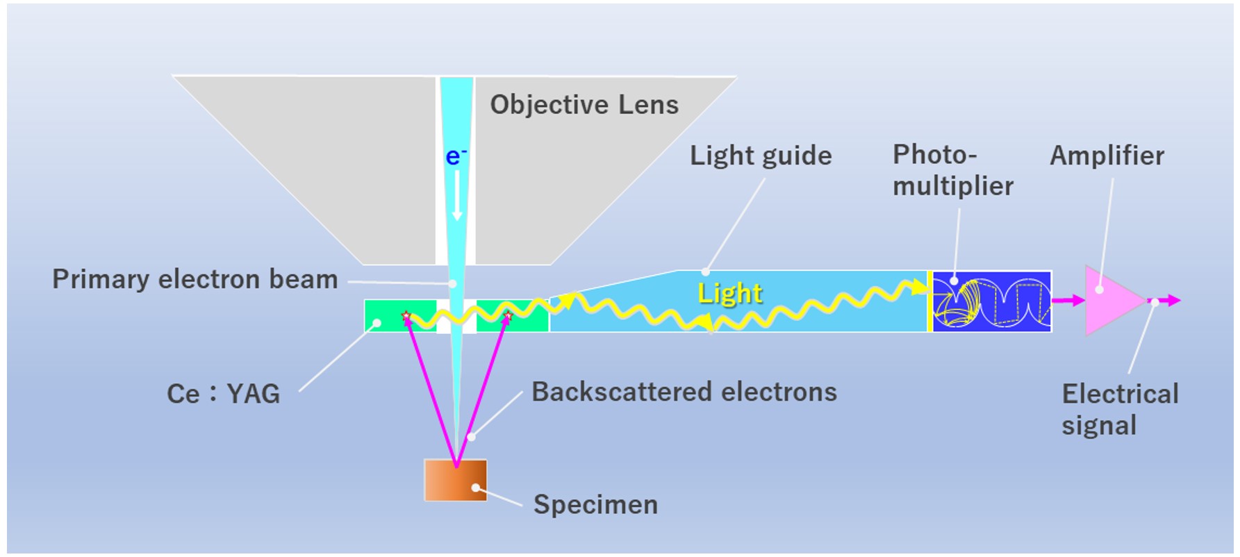
図1 YAG BSE検出器の模式図
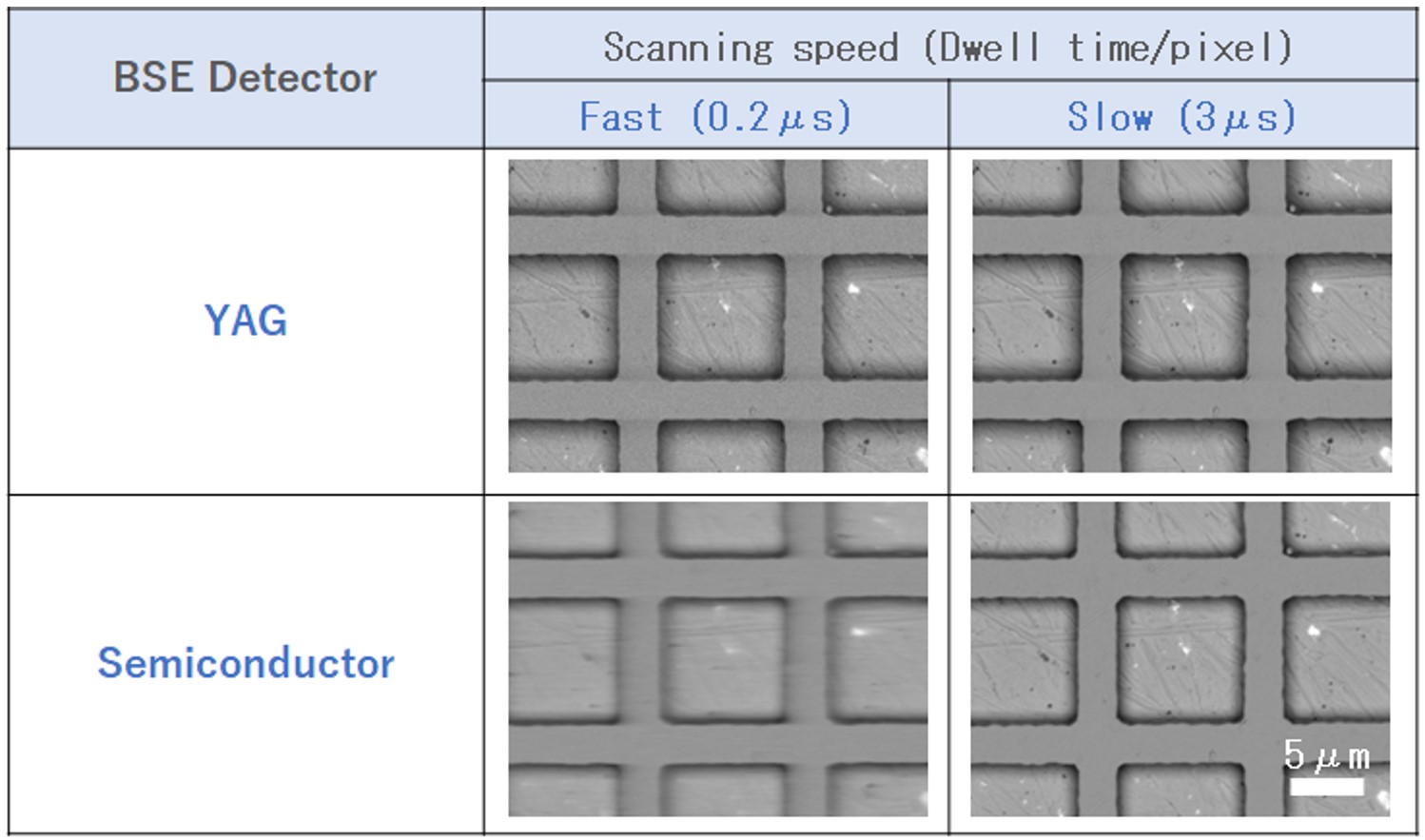
図2 反射電子像の比較。(左) 速い走査速度で取得、(右) 遅い走査速度で取得。左下の像には、速い走査で試料が横に動いたような「像のぼけ」が見られる。
A backscattered electron (BSE) detector using a crystal of Yttrium Aluminum Garnet (Y3Al5O12), abbreviated to YAG, with cerium (Ce) added as a fluorescent active material. (Here, this YAG is termed “Ce: YAG”.)
The most widely used BSE detector is the semiconductor detector. However, since the semiconductor detector has a long response time (slow response speed), a specimen image is blurred at a fast scanning speed. The YAG BSE detector is used to avoid this phenomenon.
Fig. 1 schematically shows the YAG BSE detector. Backscattered electrons, which are generated at illuminating a focused electron beam onto a specimen, travel toward a “Ce: YAG” placed just above the specimen. Then, the generated light (fluorescence light) reaches a photo-multiplier tube via a light guide. The light is converted into electrons at the photocathode and the electrons are further multiplied. The multiplied electrons reach the anode and become an electrical signal. The electrical signal is further amplified. Since “Ce: YAG” has a short attenuation time (about 70 ns) of fluorescence, the response time of the YAG BSE detector is more than one order of magnitude shorter than that of the semiconductor BSE detector.
If the response time is long, as in the case of the semiconductor BSE detector, the SEM image may be blurred as if the specimen has moved sideways when observed at a fast scanning speed (seen in the lower left image of Fig. 2). As the YAG BSE detector has a short response time, the image can be observed without blurring even at fast scanning speeds. Therefore, the image can be seen clearly even when the specimen stage is moved quickly and the desired observation position can be found without time lag. Furthermore, in the case of Array tomography, the YAG BSE detector can shorten the image acquisition time to take many images over a wide area of a specimen.
Fig. 1 Schematic of YAG BSE detector
Fig. 2 BSE images acquired in a fast scanning speed (left) and a slow scanning speed (right). Blurred image (left down) is noted, as if the specimen moved sideways at a high speed scanning.
関連用語から探す
説明に「YAG反射電子検出器」が含まれている用語


