色収差
色収差
chromatic aberration
[目次:理論]
電子線が電子レンズを通過するときに、個々の電子のエネルギーのばらつきが原因で生じる電子線の広がり。
全ての電子のエネルギーEが同じ(単色)電子線は、他の収差がなければ、焦点面上の一点に集束する。しかし、電子のエネルギーにばらつきがあると、エネルギーの大小によって電子線の集束位置が焦点面の前後にずれて、一点に集束しない。その様子を図1に示す。エネルギーEの電子の軌道を黒で、エネルギーEに対してΔE/2だけ大きいエネルギーの電子の軌道を青で、ΔE/2だけ小さいエネルギーの電子の軌道を赤で示す。エネルギーEに対して±ΔE/2のエネルギーのばらつきがある場合、焦点面上での電子プローブの最小の直径(最小錯乱円の直径)dcは、dc = CcαΔE/Eと与えられる。※1 ここで、αはエネルギーEの電子線に対する集束半角、Ccは対物レンズの色収差係数(chromatic aberration coefficient)と呼ばれ、ΔE/Eの比例係数である。Ccは対物レンズと試料の間の距離(working distance、WD)の関数で、図2に示すようにWDの増加に対して、単調に増加する。
エネルギーのばらつきの幅ΔEは、電子銃のタイプによって異なる。タングステンフィラメントを用いた熱電子銃のΔEは1~3 eV、ショットキーエミッション型電子銃のΔEは0.5 eV、冷陰極電界放出型電子銃のΔEは0.3~0.4 eVである。一般的なSEMの加速電圧は0.5 kV~30 kVであり、加速電圧が低いほど色収差は大きくなり、電子プローブの直径dcは増大する。 アウトレンズ型の対物レンズでは、WDを約10 mmで用いることが多い。その場合、Ccとαをそれぞれ20 mmと5 mrad、タングステンフィラメントの熱電子銃のΔEを1 eVとすると、加速電圧が20 kVのとき、dcは5.0 nmと算出される。
※1 L. Reimer, Scanning Electron Microscopy, Springer, Berlin, Germany, p. 24 (1998).
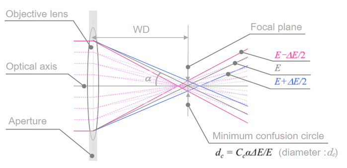
図1.電子レンズの色収差に起因する電子線の広がり
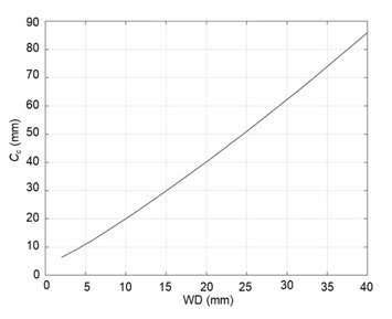
図2.対物レンズと試料の間の距離(WD)と色収差係数Ccの関係
The chromatic aberration causes a spread of electron beams on the focal plane of the objective lens due to the difference in the focal positions for the electron beams with different energies.
The monochromatic electron beams having the same energy E converge onto a point of the focal plane of the objective lens. However, if the electron beams have an energy spread, the beams do not converge on one point but converge on front or rear the focal plane depending on the energy difference ±ΔE, as is shown schematically in Fig. 1. The tracks of the electron beams with energy E, with energy E+ΔE/2, and with energy E–ΔE/2, are respectively drawn by black, blue and red lines. When the energy spread is ±ΔE/2 with respect to E, the smallest diameter dc (minimum confusion circle) of the electron probe on the focal plane is given by dc = CcαΔE/E.
Here, α is the convergence semi-angle of the electron beam with energy E, and Cc is the proportional factor of ΔE/E, called "chromatic aberration coefficient" of the objective lens. Cc is a function of the distance between the objective lens and specimen (working distance, WD). As shown in Fig. 2, Cc monotonically increases with increasing WD.
The energy spread ΔE is different for the types of the electron gun of the SEM instrument. For a thermionic-emission electron gun with a tungsten filament, ΔE is 1 to 3 eV. For a Schottky emission electron gun, ΔE is 0.5 eV. For a cold field-emission electron gun (CFEG), ΔE is 0.3 to 0.4 eV. The accelerating voltage of an ordinary SEM ranges between 0.5 kV and 30 kV. As the accelerating voltage is lower, the chromatic aberration becomes larger, giving to a larger electron probe diameter dc.
In the out-lens type objective lens, WD is usually set at about 10 mm. When Cc and α are assumed respectively as 20 mm and 5 mrad, dc is calculated to be 5.0 nm at an energy spread ΔE = 1 eV for the tungsten filament of the thermionic-emission electron gun.
※1 L. Reimer, Scanning Electron Microscopy, Springer, Berlin, Germany, p. 24 (1998).
Fig. 1 Schematic diagram of the spread of electron beams due to chromatic aberration of the objective lens
Fig. 2 Relationship between the working distance WD and chromatic aberration coefficient Cc
関連用語から探す
説明に「色収差」が含まれている用語


