球面収差
球面収差
spherical aberration
[目次:理論]
電子線が電子レンズを通過するときに、光軸に近いところを通過する電子と、光軸から遠いところを通過する電子の集束する位置の違いが原因で生じる電子線の広がり。
図1に示すように、光軸に平行でレンズの中心部(光軸)に近い軌道を通る電子はレンズの焦点面で光軸上に集束する。しかし、光軸から遠い軌道を通る電子は、焦点面よりもレンズに近い位置で光軸と交わる。そのため、焦点面上で電子は広がる。この広がりの直径は2Csα3となる。ここでCsは対物レンズの球面収差係数(spherical aberration coefficient)、αは電子線の集束半角である。Csは対物レンズと試料の間の距離(working distance、WD)の関数であり、図2に示すようにWDの増加に対して、単調に増加する。電子プローブは焦点面よりレンズに近い位置で最小になり、その位置での直径は最小錯乱円と呼ばれる。最小錯乱円の直径dsはds = Csα3/2で表される。※1 アウトレンズ型の対物レンズでは、対物レンズと試料の間の距離(Working distance)を10 mm程度で、加速電圧を15 kVで用いることが多い。この場合、Csとαをそれぞれ50 mmと5.0 mradとすると、ds = 3.1 nmと算出される。
※1 L. Reimer, Scanning Electron Microscopy, Springer, Berlin, Germany, p. 24 (1998).
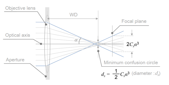
図1.電子レンズの球面収差に起因する電子線の広がり。
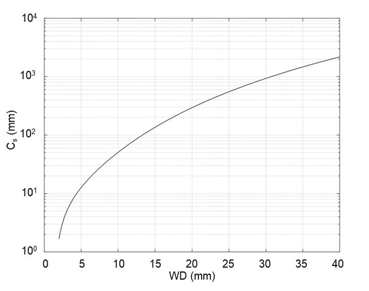
図2.対物レンズでの試料の間の距離(WD)と球面収差係数Csの関係
The spherical aberration causes a spread of electron beams on the focal plane of the objective lens due to the difference in the focal positions between the electron beams passing near the optical axis and the electron beams passing away from the optical axis.
As shown in Fig. 1, the electron beams parallel to the optical axis and passing near the center (near the optical axis) of the objective lens intersect with the optical axis on the focal plane of the lens. However, the electron beams tracking away from the optical axis intersect with the optical axis at positions closer to the lens than the focal plane. This feature results in a spread of the electron beams on the focal plane. The diameter of the spread is given by 2Csα3, where Cs is the spherical aberration coefficient of the objective lens and α is the convergence semi-angle of the electron beam. Cs is a function of the distance between the objective lens and specimen (working distance, WD). As shown in Fig. 2, Cs monotonically increases with increasing WD. The electron probe becomes smallest at a point a little near the lens from the focal plane. The diameter of the electron probe at this point is called "minimum confusion circle" (ds), expressed as ds = Csα3/2.
The SEM instrument equipped with an out-lens objective lens is normally used with a WD of about 10 mm and at an accelerating voltage of 15 kV. In such a case, ds is calculated to be 3.1 nm, when Cs and α are assumed respectively as 50 mm and 5.0 mrad.
※1 L. Reimer, Scanning Electron Microscopy, Springer, Berlin, Germany, p. 24 (1998).
Fig. 1 Schematic diagram of the spread of electron beams due to the spherical aberration of the objective lens.
Fig. 2 Relationship between the working distance (WD) and spherical aberration coefficient Cs for an objective lens.
関連用語から探す
説明に「球面収差」が含まれている用語


