二次電子像
二次電子像
secondary electron image, SE image
[目次:理論]
入射電子(一次電子)が試料内で非弾性散乱することによって、試料を構成する原子から励起された二次電子を検出することで作られる像。通常SEM像とは二次電子像のことであり、試料表面の微細な構造を知ることができる。二次電子のエネルギーは数10 eV以下であるため、表面から5 - 10 nmの深さから発生したもののみが真空中へ放出される。そのため、空間分解能が高く、試料の最表面構造に敏感である。ただし、エネルギーが低いので、試料表面の帯電の影響による像の乱れが生じやすい。
入射電子線に対する試料表面の傾斜角が大きいと、試料表面からの二次電子の放出が大きいので、試料の形状に依存したコントラストがつく。さらに、試料表面の小さな突起やシャープな凹凸の部分からは、二次電子の放出が顕著に増大し、像にさらなる明るいコントラストを形成する。これは、エッジ効果と呼ばれる二次電子像に特有なコントラストで、微細な構造が鮮明に観察できる。
図(a)に三酸化タングステン結晶の二次電子像を示す。結晶の表面の傾きによって放出される二次電子の量が異なり、結晶の形状を知ることができる。エッジの部分が特に明るくなっており、エッジ効果が確認できる。
分解能は、加速電圧が15 kVで、0.6nm~3nm程度である。分解能を決める主たる因子は、入射電子のプローブ径である。電子銃にはタングステンやLaB6が用いられるが、より小さなプローブ径を得るには、より光源の小さい電界放出型電子銃が使われる。 鮮明な像を得るには加速電圧を低くすることが有効である。低加速電圧では、入射電子の試料内への拡散が小さく、表面付近で励起された二次電子によって像が作られ、試料表面の微細な構造を鮮明に見ることができる。高加速電圧では、入射電子の拡散領域が大きくなり、入射電子から隔たったところから発生する二次電子の寄与があり、微細な構造は見にくくなる。加速電圧を下げると、対物レンズの収差が大きくなり、プローブ径が大きくなる。しかし、対物レンズの改良により、現在のSEMでは加速電圧5kVでも十分小さなプローブ径が得られている。
図(b)に、金をコートした濾紙を加速電圧5 kVと30 kVとで観察した二次電子像を示す。加速電圧5 kV では、コントラストが高く、表面構造が鮮明に見えている。加速電圧30 kV では、コントラストが低下し、表面構造の詳細が不鮮明である。
図(a) 三酸化タングステン結晶の二次電子像 (加速電圧:10 kV)⇒図
図(b) 加速電圧の違いによる二次電子像(同一視野)の比較。⇒図
試料:金コートした濾紙、加速電圧: 5 kV(写真左)、30 kV(写真右)。表面構造の観察には低加速電圧の方が適している。
“Secondary electron image” means an image formed by detecting secondary electrons which are generated from the constituent atoms excited by inelastic scattering of the incident (primary) electrons in a specimen. An SEM image generally indicates a secondary electron image, and the image reveals fine surface structures (topographic details) of the specimen. Since the energy of the secondary electron is several 10 eV or less, only the electrons generated within 5 to 10 nm from the surface are emitted in vacuum, beyond the specimen. Thus, the secondary electron image provides high spatial-resolution and is very sensitive to the top-surface structure of the specimen. However, since the energy of the secondary electron is low, image blur is likely to arise, caused by a charging on the specimen surface.
Increasing the specimen tilt angle increases the emission amount of secondary electrons beyond the specimen surface, thus producing contrast depending on the specimen shape. Furthermore, from small protrusions or sharp topographic regions on the specimen, the emission amount of the secondary electrons increases remarkably, leading to further brighter contrast of the image. This contrast is called the edge effect characteristic of the secondary electron image and enables clear observation of the fine surface structure.
Fig. (a) shows a secondary electron image of crystalline particles of trioxide tungsten. The image reveals the shape of the crystalline particles due to the different emission amount of secondary electrons caused by different inclination of the surfaces of crystalline particles. The edge regions are seen to be particularly bright (edge effect) while the edge effect is confirmed.
The image resolution is 0.6 nm to 3 nm for an accelerating voltage of an incident electron probe of 15 kV. The main factor that determines the resolution is the diameter of the incident electron probe. W (tungsten) or LaB6 is normally used for the electron source (gun). To obtain a smaller electron-probe diameter, a field emission gun (FEG) that has a smaller electron source is used.
For observing a clear image, it is effective to decrease the accelerating voltage. At low accelerating voltages, the diffusion region of the incident electrons into the specimen is small. Thus, the image is formed by secondary electrons excited near the surface, resulting in clear imaging of the fine surface structure of the specimen. However, when the accelerating voltage is lowered, the chromatic aberration of the electron lens increases, leading to the degradation of the resolution. Thus, to use a lens with a small aberration is desirable. To the contrary at high accelerating voltages, the diffusion region of the incident electrons becomes large, and thus, the contribution of the secondary electrons generated in a region distant from the incident electron path becomes large. As a result, the obtained image becomes unclear and the fine surface structure of the specimen is difficult to view. Decreasing the accelerating voltage increases the aberration of the objective lens and the probe diameter becomes large. But in the present SEM, the improvement of the objective lens enables a sufficiently small probe diameter to be obtained even at an accelerating voltage of as low as 5 kV.
In Fig. (b), two secondary electron images are compared, where a gold-coated filter paper is observed at accelerating voltages of 5 kV and 30 kV, respectively. At a voltage of 5 kV, the image shows high contrast and the surface structure is clearly observed. At a voltage of 30 kV, the image is degraded and the details of the surface structure are unclear.
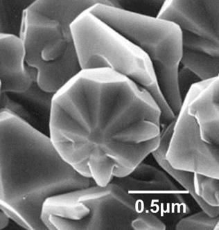
Fig. (a) Secondary electron image of crystalline particles of trioxide tungsten, taken at an accelerating voltage of 10 kV.
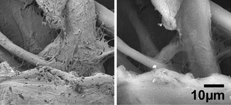
Fig. (b) Comparison of secondary electron images (same field of view) of a gold-coated filter paper taken at accelerating voltages of 5 kV (left) and 30 kV (right).
Low accelerating-voltage is suitable for observation of fine surface structure (topographic details).
関連用語から探す
説明に「二次電子像」が含まれている用語


