反射電子検出器
反射電子検出器
backscattered electron detector, BE detector, BSE detector, BED, BE, BSE
[目次:装置]
最も広く使われる反射電子検出器はシリコン半導体検出器である。この検出器を用いると試料の組成像や凹凸像を得ることができる。(日本電子製SEMの中には、基本操作画面(UI)上に組成像をBED-C、凹凸像をBED-Tと区別して表示しているものもある)
この検出器は薄板で、通常、円環状に整形されており、円環(アニュラー)型反射電子検出器と呼ばれる。対物レンズの直下に設置する。入射電子は検出器の中央の穴の部分を通る(図1)。反射電子はエネルギーが高いので、直進して検出器に入射する。そのため、二次電子の場合のように検出器に電圧をかけて電子を収集する必要がない。
反射電子検出器は薄いので、元素分析のためのEDS検出器の挿入に支障をきたさず、組成像および凹凸像の観察と元素分析を同時に行うことができる。その他のオプション検出器(波長分散型X線分光器(WDS)/軟X線発光分光器(SXES))も同時に作動することができる。なお、二次電子検出器(ET検出器)を同時に使用できる。高倍率での観察を行う場合には、試料を対物レンズに近づける必要があり、作動距離は3 mm未満にせざるを得ない。そのため、反射電子検出器自身を一時的に退避(リトラクト)できる構造をとることが多い。
シリコン半導体の円環型反射電子検出器には2分割、4分割、さらに多くの部分に分割されているものもあるが、主流は4分割である。ここでは説明のための例として2分割した検出器を図1に示す。2分割した検出器(図1のAおよびB)を用いた場合、二つの出力信号を加算することにより試料の組成像を得ることができ、減算することにより試料の凹凸像を得ることができる。
円環型反射電子検出器に加えて、試料から見て低い角度に反射された電子を検出する第2の半導体検出器を備えた装置もある(図1のC)。この第2の検出器で低角に反射された電子のみを検出すると、試料を斜め方向から照明した効果が強調され、陰の部分が大きく(長く)なって、より立体感に富んだ反射電子像が得られる。(日本電子製SEMの中には、基本操作画面(UI)上にBED-Sと区別して表示しているものもある。)
高分解能SEMでは、検出器を鏡筒内部にも配置し、対物レンズの中を通過した反射電子を検出することもある(図1のD)。この方式では、入射電子の方向に近い高角度に反射された電子のみが検出され、試料の凹凸情報を含まない組成情報のみの信号が得られる。
シリコン半導体検出器が反射電子検出器として主流であるが、応答速度に劣るという欠点がある。応答速度に優れた反射電子検出器として、イットリウム・アルミニウム・ガーネット(YAG)を代表とするシンチレーターを用いた検出器を使用することもある。ただし、シンチレーター型検出器は分割した形状をとることが難しい。そのため、多分割した検出器を利用した試料の凹凸像は得られない。
半導体検出器の原理
半導体検出器の原理は以下のとおりである(図2)。検出器用の半導体には、SiのP層とN層の接合からなるPN型フォトダイオードを用いる。図2に示すように、P層とN層の接合部には空乏層と呼ばれる伝導電子・正孔が存在しない領域がある.検出器に反射電子が入ると、空乏層中で電子・正孔対が励起され、P層とN層の間に存在する電位差によって電子はN層へ、正孔はP層に流れる。この電流を増幅して反射電子像の形成に用いる。
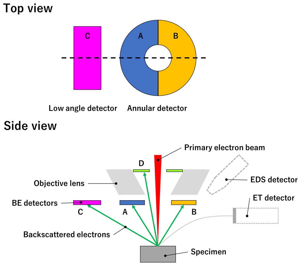
図1 シリコン半導体反射電子検出器の配置の模式図。
円環(アニュラー)型反射電子検出器(AとB),低角度検出器C及び鏡筒内反射電子検出器D。上図は検出器を上方から見た形状。下図は、上の図の破線部分を横方向から見たときの検出器の配置を示す。試料、対物レンズ、二次電子検出器、EDS検出器、および入射電子線と反射電子線を描き加えている。反射電子の量は試料面に垂直な方向に向かって多くなる。そのため,凹凸を含んだ試料を観察すると試料面の向きが局所的に変わるので、分割された二つの検出器AとBで検出される反射電子の信号量に差が生じる。そこで、AとBからの信号を加算(A+B)すると凹凸が消え、試料の組成を表す像(組成像)が得られる。一方、AからBの信号を減算(A-B)すると試料の凹凸が強調される(凹凸像)。試料から反射された電子の中で、低角度に反射されたものを検出器Cで検出した信号を組成像(A+B)に加算(A+B+C)すると、斜め照明の効果がより強くなり、陰の部分が大きく(長く)なって、より立体感に富んだ像が得られる。
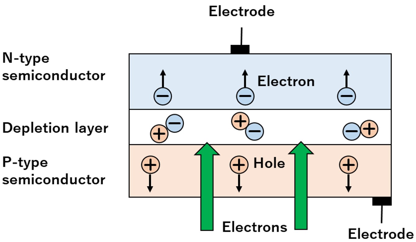
図2 PN型フォトダイオードに反射電子が入射したときの動作の概念図
The most widely used backscattered electron (BE) detector is a silicon (Si) semiconductor detector. The detector enables us to obtain the compositional image and the topographic image of a specimen. (Some JEOL SEMs display the compositional image as BED-C and the topographic image as BED-T on the monitor screen.
The BE detector is usually made of an annular-shaped thin plate and called the annular BE detector. The detector is placed just below the objective lens. The incident electrons pass through the center hole of the detector (Fig. 1). Since the backscattered electrons have high energies, they travel straight and come to the detector. Thus, it is not necessary to apply a voltage to the detector for collecting the electrons, unlike the case of secondary electrons.
As the BE detector is thin, it does not interfere insertion of an energy-dispersive X-ray spectroscopy (EDS) detector for elemental analysis into the microscope column, enabling observation of the compositional and topographic images and analysis of the constituent elements simultaneously. Not only a secondary electron detector (ET detector) but also the other optional detectors, a wavelength-dispersive X-ray spectrometer (WDS) and/or a soft X-ray emission spectrometer (SXES), can also be installed together with the BE detector and operated simultaneously. For high-magnification observation, the specimen is needed to bring close to the objective lens and the working distance (WD) must be less than 3 mm resulting in overlap of the specimen and the detector. Thus, the BE detector is often constructed to be temporarily retractable from the microscope column.
The Si semiconductor annular BE detectors include two-segmented type, four-segmented type and more-segmented type. Among them, the four-segmented detector is mainly used. For convenience, Fig. 1 illustrates a two-segmented detector as an example. In a two-segmented detector (A and B in Fig. 1), the compositional image can be obtained by adding the output signals from the two segments, and the topographic image can be obtained by taking difference between the two signals.
There are SEM instruments equipped with the second semiconductor detector to detect the electrons backscattered at low angles viewed from the specimen (C in Fig. 1), in addition to the above-mentioned annular BE detector. If the electrons backscattered only at low angles are detected by this second detector, the shadowing effect, an effect of illuminating specimen from an oblique direction, is enhanced or the shaded area becomes larger (longer), resulting in an image with a more three-dimensional effect. (Some JEOL SEMs display the shadow image as BED-S on the monitor screen.
High-resolution SEMs, in some cases, employ an additional detector placed inside the microscope column (D in Fig. 1). This detector allows to detect only the electrons backscattered at high angles near the direction of the incident electrons, making it possible to acquire only the compositional image without topographic nature.
If a high-speed response for backscattered electron signals is needed, a high-response-speed detector like an yttrium aluminum garnet (YAG) scintillator detector can be used instead of the BE detector. It is however noted that the scintillator detector is difficult to form segment-shaped, and thus not possible to emphasize or erase the topographic image, which can be performed by the BE detector.
Principle of the Si semiconductor detector
The principle of the semiconductor detector is as follows (illustrated in Fig. 2). The detector uses a PN-type photodiode, which consists of a junction of a “P” layer and an “N” layer of Si. The “depletion layer”, where conduction electrons and holes do not exist, is formed at the junction of the P layer and the N layer. When backscattered electrons enter the detector, electron-hole pairs are created in the depletion layer. Then, the potential difference between the P layer and the N layer causes the electrons to flow to the N layer and the holes to the P layer. The electric current due to the flow of those electrons and holes is amplified and used to form a backscattered electron image.
Fig. 1. Schematics of arrangements of the Si semiconductor BE detectors.
The annular BE detector (pair of A and B), the low-angle detector C, and the in-column BE detector D. The upper figure is the top view of the detectors. The lower figure shows the side view of the arrangement of the detectors along the dotted line in the upper figure relative to the objective lens, the specimen, the SE (secondary electron) detector and the EDS detector (including the incident electron path and the backscattered electron path).
The backscattered electrons increase towards the direction perpendicular to the specimen surface. When the specimen surface is uneven, the backscattered electron intensities detected by the detectors A and B are different. If the signals from A and B are added (A+B), the compositional image is obtained with erasing the topographic image. If the signal B is subtracted from signal A, (A–B), the topographic image is obtained with an emphasis. When the electrons backscattered at low angles detected by the detector C are added to the compositional image (A+B+C), a strong shadowing effect arises, that is the shaded area becomes long, or a three-dimensional effect is enhanced.
Fig. 2. Conceptual diagram of the action of the PN-type photodiode when electrons are incident on it.
関連用語から探す
説明に「反射電子検出器」が含まれている用語


