反射電子像
反射電子像
backscattered electron image, BSE image
[目次:理論]
入射電子の弾性散乱によって放出された反射電子 (後方散乱電子) によって作られる像。試料の組成の違い (平均原子番号の差) を知ることができる。空間分解能は二次電子像には劣る。二次電子像で見られるエッジコントラストは見られない。また、エネルギーが高いため、試料表面の帯電の影響を受けにくい。
原子番号が約40以下では、反射電子放出率の変化が大きいので、わずかな原子番号差でもコントラストが付く。例えば、原子番号が30付近では、平均原子番号の差が0.2~0.3あれば十分なコントラストが付き識別できる。具体的には、29 (Cu) と30 (Zn) の化合物の真鍮や、31 (Ga) と33 (As) の化合物半導体で、それぞれの原子が識別できる。
通常、反射電子像の分解能は、二次電子像に比べて数倍~1桁程度悪くなる。その理由は、二次電子は表面から深さ10 nm程度の間から放出するのに対して、反射電子は表面から数 um (入射電圧に依存) の間から放出するため、試料表面に到達するまでに大きく拡散するためである。ただし、近年の高分解能SEMでは、入射電子のエネルギーが1kV以下での反射電子の検出が可能になっており、反射電子の拡散領域がきわめて小さく抑えられ、反射電子像の分解能は、同じ入射電子エネルギーで得られた二次電子像の分解能と差がない。
また、反射電子像から試料表面の凹凸の様子を知ることができる。凹凸のある試料を観察すると、凹凸の片側に影がつき、立体感のある像が得られ、凹凸の判定に有効である。ただし、反射電子の拡散効果によって、二次電子像のようなエッジを強調した像 (エッジ効果) は作られない。
図 (a) に、名刺に印刷された文字の部分の二次電子像と反射電子像を示す。文字のインクには重金属が含まれるため、反射電子像では紙の繊維部分に比べて明るいコントラストが現われている (組成コントラスト )。二次電子像では組成コントラストは見られない。ただし、試料には、チャージアップを避けるために表面にカーボンのコーティングが施されている。
図 (b) に、カードエッジコネクターの電極表面の二次電子像と反射電子像を示す。二次電子像では凹凸の程度が分かりにくいが、反射電子像では強い斜め照明の効果によって凹凸の高低をしっかりと把握することができる。
組成が均一な結晶性試料では、結晶の方位の違いが反射電子の放出に影響し、電子チャンネリングコントラストと呼ばれるコントラストが現われる。
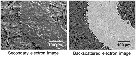
二次電子像 (左) と反射電子像 (組成コントラスト) (右) の対比
加速電圧: 15 kV, 試料: カーボンコートした名刺の文字部分 (中央)
反射電子像では文字部分が非常に明るくなっている。
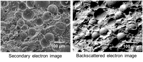
二次電子像と反射電子像 (凹凸コントラスト) の対比
試料: カードエッジコネクターの電極, 加速電圧: 10 kV
反射電子像では強い斜め照明の効果によって凹凸の高低が明瞭に見える。
"Backscattered electron image" means an image formed by backscattered (reflected) electrons which are emitted by elastic scattering of the incident (primary) electrons. A backscattered electron image reveals the compositional difference in a specimen (difference in the average atomic number). Its spatial resolution is low in comparison with that of the secondary electron image. The edge contrast does not occur, which appears in the secondary electron image. The backscattered electron image is less affected by electric charging on the specimen surface than the secondary electron image because the backscattered electrons have a high energy.
The backscattered electron emission rate (coefficient) greatly changes for the atoms with an atomic number up to 40. Thus, the backscattered electron image is sensitive to a small difference of atomic number for a specimen with such atomic numbers. For example, for a specimen with an atomic number near 30, if the difference in average atomic number is more than 0.2 to 0.3, a sufficient difference in the image contrast can be recognized. Specifically, each atom can be identified for brass composed of Cu (29) and Zn (30), and for a compound semiconductor of Ga (31) and As (33).
In general, the spatial resolution of the backscattered electron image is worse than that of the secondary electron image, namely several times to one order of magnitude lower. The reason for this is as follows. Although secondary electrons are emitted from a small depth of only 10 nm from the surface, the backscattered electrons are emitted from a large depth of a few micrometers from the surface (depending on the accelerating voltage of the incident beam). This gives rise to a large diffusion for the backscattered electrons until to reach the specimen surface, resulting in a low resolution. However, the recent high-resolution SEM enables the detection of backscattered electrons even for the incident electron energy as low as 1keV or less. Thus, the diffusion region of the backscattered electrons is suppressed extremely small, and then, the backscattered electron image produces a high resolution comparable to that of the secondary electron image taken by the same incident electron energy.
The backscattered electron image also shows the topography of the specimen surface. When an uneven specimen is observed, a shadow is produced on one side of a tilted face, enabling acquisition of a stereoscopic (shadow) image.
However, an edge-emphasized image formed by secondary electrons cannot be obtained due to the diffusion effect of the backscattered electrons.
Fig. (a) shows a set of a secondary electron image and a backscattered electron image of the letter-printed part on a name card. Since the ink of letters contains heavy metals, the backscattered electron image shows a brighter contrast than that of the fiber part of the name card (compositional contrast). The compositional contrast is not seen in the secondary electron image. It is noted that, the surface of this specimen is carbon-coated to avoid electric charging.
Fig. (b) shows a set of a secondary electron image and a backscattered electron image of the surface of an electrode of a card-edge connector. The backscattered electron image reveals the specimen topography stereoscopically owing to a strong oblique illumination effect. It should be noted that the secondary electron image does not show the stereoscopic contrast.
It is noted in addition, for a crystalline specimen with a uniform composition, the backscattered electron image shows so-called the electron channeling contrast due to a difference in crystal orientation.
Fig. (a) Comparison of a secondary electron image (left) and a backscattered electron image (right) of the letter part of a carbon-coated name card (seen at the center of both images), taken at an accelerating voltage of 15 kV.
In the backscattered electron image, the letter part appears very bright (compositional contrast).
Fig. (b) Comparison of a secondary electron image (left) and a backscattered electron image (right) of the surface of an electrode of a card-edge connector, taken at an accelerating voltage of 10 kV.
In the backscattered electron image, topographic details of the specimen are stereographically observed owing to a strong oblique illumination effect (topographic contrast).
関連用語から探す
説明に「反射電子像」が含まれている用語


